GPGPUs and their programming
Sima, Dezső
Szénási, Sándor
GPGPUs and their programming
írta Sima, Dezső és Szénási, Sándor Szerzői jog © 2013 Typotex
Kivonat
The widespread use of GPGPUs in an increasing number of HPC (High Performance Computing) areas, such as scientific, engineering, financial and business applications, is one of recent major trends in using informatics.
The lecture slides worked out pursuit two goals. On the one side the lecture aims at presenting the principle of operation, the microarchitecture and main features of GPGPU cores, as well as their implementation as graphics cards or data parallel accelerators. On the other hand, the practical part of the lectures aims at acquainting students with data parallel programming, first of all with GPGPU programming and program optimization using the CUDA language and programming environment.
Tartalom
I. GPGPUs ... 1
Aim ... ix
1. Introduction to GPGPUs ... 10
1. Representation of objects by triangles ... 10
1.1. Main types of shaders in GPUs ... 11
2. Convergence of important features of the vertex and pixel shader models ... 12
3. Peak FP32/FP64 performance of Nvidia’s GPUs vs Intel’ P4 and Core2 processors [7] 14 4. Peak FP32 performance of AMD’s GPUs [8] ... 15
5. Evolution of the FP-32 performance of GPUs [9] ... 16
6. Evolution of the bandwidth of Nvidia’s GPU’s vs Intel’s P4 and Core2 processors [7] 16 7. Comparing main features of CPUs and GPUs [12] ... 17
2. The virtual machine concept of GPGPU computing ... 19
1. Introduction to the virtual machine concept of GPGPU computing ... 19
1.1. The virtual machine concept as used for GPGPUs ... 19
1.2. Benefits of the portability of the pseudo assembly code ... 19
1.3. The process of developing applications-1 ... 19
1.4. The process of executing applicatons-2 ... 20
1.5. Formulation of application programs at different levels of abstraction ... 20
2. Introduction to a GPGPU-based massively data parallel computational model ... 21
2.1. Specification of GPGPUs at different levels of abstraction ... 21
2.2. Specification of the GPGPU virtual machine ... 22
2.3. The GPGPU-based massively data parallel computational model ... 22
2.4. Emergence of GPGPU-based massively data parallel computational models 22 2.5. The choice of the computational model presented ... 23
2.6. The choice of the terminology used ... 23
2.6.1. Designation of the GPGPU-based massively data parallel computational model as the SIMT (Single instruction Multiple Threads) model of computation 23 2.6.2. Designation of the terms related to GPGPU-based massively data parallel computational model ... 23
3. Introduction to the SIMT computational model ... 24
3.1. Main components of the SIMT computational models ... 24
3.2. The model of the compute workload ... 24
3.2.1. The thread model ... 25
3.2.2. The kernel concept ... 29
3.3. The model of the platform ... 31
3.3.1. The model of computational resources ... 31
3.3.2. The memory mode ... 35
3.4. The execution model ... 39
3.4.1. The concept of SIMT execution ... 39
3.4.2. The concept of assigning work to the PEs ... 43
3.4.3. The concept of data sharing ... 47
3.4.4. The concept of data dependent flow control ... 48
3.4.5. The concept of synchronization ... 50
4. The Pseudo ISA of GPGPU computing ... 51
4.1. Discussion of pseudo ISAs ... 52
4.2. Case example: The pseudo ISA of Nvidia’s PTX virtual machine ... 52
4.3. Case example: The pseudo ISA of Nvidia’s PTX virtual machine ... 53
4.4. Nvidia’s compute capability concept [31], [1] ... 54
4.5. a) Evolution of the functional features, called compute capabilities in subsequent versions of Nvidia’s pseudo ISA (PTX) [32] ... 55
4.6. b) Evolution of the device parameters bound to subsequent compute capability versions of Nvidia’s PTX [32] ... 55
4.7. c) Architecture specifications bound to compute capability versions of Nvidia’s PTX [32] ... 56
4.8. d) Throughput of native arithmetic instructions in subsequent compute capability
versions of Nvidia’s PTX (operations per clock cycle/SM) [7] ... 56
4.9. PTX ISA Versions generated by subsequent releases of CUDA SDKs and supported compute capability versions (sm[xx]) (designated as Supported Targets in the Table) [20] ... 57
4.10. Compute capability versions supported by Nvidia’s GPGPU cores and cards [32] 58 4.11. Forward portability of PTX code [31] ... 58
4.12. Compatibility rules of object files (CUBIN files) compiled to a particular GPGPU compute capability version [31] ... 58
3. Overview of GPGPU cores and cards ... 59
1. General overview ... 59
1.1. GPGPU cores ... 59
1.2. Main features of Nvidia’s dual-GPU graphics cards ... 62
1.3. Main features of AMD’s/ATI’s dual-GPU graphics cards ... 62
1.4. Remarks on AMD-based graphics cards [36], [37] ... 62
2. Overview of the main features of Nvidia’s graphics cores and cards ... 63
2.1. Main features of Nvidia’s graphics cores and cards ... 63
2.1.1. Structure of an SM of the G80 architecture ... 64
2.1.2. Positioning Nvidia’s GPGPU cards in their entire product portfolio [41] 67 2.2. Examples for Nvidia’s graphics cards ... 68
2.2.1. Nvidia GeForce GTX 480 (GF 100 based) [42] ... 68
2.2.2. A pair of Nvidia’s GeForce GTX 480 cards [42] (GF100 based) .... 68
2.2.3. Nvidia’s GeForce GTX 480 and 580 cards [44] ... 69
2.2.4. Nvidia’s GTX 680 card [80] (GK104 based) ... 70
2.2.5. Nvidia’s GTX Titan card [81] (GK110 based) ... 70
3. Overview of the main features of AMD’s graphics cores and cards ... 71
3.1. Main features of AMD’s graphics cores and cards ... 71
3.2. Examples for AMD’s graphics cards ... 75
3.2.1. ATI HD 5970 (actually RV870 based) [46] ... 76
3.2.2. ATI HD 5970 (RV870 based) [47] ... 76
3.2.3. AMD HD 6990 (Cayman based) [48] ... 77
3.2.4. AMD Radeon HD 7970 (Tahiti XT, Southern Islands based) - First GCN implementation [49] ... 77
3.2.5. Prices of GPGPUs as of Summer 2012 [50] ... 78
4. Nvidia’s Fermi family of graphics cores and cards ... 80
1. Overview of the Fermi family ... 80
1.1. Major sub-families of Fermi ... 81
2. Key innovations of Fermi’s PTX 2.0 ... 81
2.1. Overview of PTX 2.0 ... 81
2.2. Key innovations of PTX 2.0 pseudo ISA ... 82
2.2.1. a) Unified address space for all variables and pointers with a single set of load/store instructions-1 [11] ... 82
2.2.2. a) Unified address space for all variables and pointers with a single set of load/store instructions-2 [11] ... 82
2.2.3. b) 64-bit addressing capability ... 83
2.2.4. c) New instructions to support OpenCL and DirectCompute APIs . 83 2.2.5. d) Full support of predication [51] ... 83
2.2.6. e) Full IEEE 754-3008 support for 32-bit and 64-bit FP precision .. 84
2.2.7. Supporting program development for the Fermi line of GPGPUs [11] 84 3. Major innovations and enhancements of Fermi’s microarchitecture ... 84
3.1. Major innovations ... 84
3.2. Major enhancements ... 84
3.3. Major architectural innovations of Fermi ... 85
3.3.1. a) Concurrent kernel execution [52], [18] ... 85
3.3.2. b) True two level cache hierarchy [11] ... 85
3.3.3. c) Configurable shared memory/L1 cache per SM [11] ... 86
3.3.4. d) ECC support [11] ... 87
3.4. Major architectural enhancements of Fermi ... 87
3.4.1. a) Vastly increased FP64 performance ... 88
3.5. Throughput of arithmetic operations per clock cycle per SM [13] ... 88
3.5.1. b) Greatly reduced context switching times [11] ... 88
3.5.2. c) 10-20 times faster atomic memory operations [11] ... 89
4. Microarchitecture of Fermi GF100 ... 89
4.1. Overall structure of Fermi GF100 [18], [11] ... 89
4.2. High level microarchitecture of Fermi GT100 ... 89
4.3. Evolution of the high level microachitecture of Nvidia’s GPGPUs [52] ... 90
4.4. Layout of a Cuda GF100 SM [19] ... 91
4.5. Evolution of the cores (SMs) in Nvidia’s GPGPUs -1 ... 91
4.6. Further evolution of the SMs in Nvidia’s GPGPUs -2 ... 93
4.7. Structure and operation of the Fermi GF100 GPGPU ... 94
4.7.1. Layout of a Cuda GF100 SM [19] ... 94
4.7.2. A single ALU (“CUDA core”) ... 95
4.8. Principle of the SIMT execution in case of serial kernel execution ... 96
4.9. Principle of operation of a Fermi GF100 GPGPU ... 96
4.10. Subtasks of work scheduling ... 96
4.11. Scheduling kernels to SMs [25], [18] ... 97
4.12. Scheduling thread blocks associated with the same kernel to the SMs ... 97
4.13. The notion and main features of thread blocks in CUDA [53] ... 98
4.14. Segmenting thread blocks into warps [59] ... 99
4.15. Scheduling warps for execution in SMs ... 100
4.16. Assumed principle of operation-1 ... 102
4.17. Assumed principle of operation-2 ... 103
4.18. Assumed principle of operation-3 ... 104
4.19. Example: Throughput of arithmetic operations per clock cycle per SM [13] 106 4.20. Scheduling policy of warps in an SM of Fermi GF100-1 ... 107
4.21. Scheduling policy of warps in an SM of Fermi GT100-2 ... 108
4.22. Scheduling policy of warps in an SM of the G80 indicating coarse grain warp scheduling ... 109
4.23. Scheduling policy of warps in an SM of the G80 indicating fine grain warp scheduling ... 109
4.24. Estimation of the peak performance of the Fermi GF100 -1 ... 110
4.25. Estimation of the peak performance of the Fermi GF100 -2 ... 112
5. Microarchitecture of Fermi GF104 ... 114
5.1. Available execution resources per SM in the GF104 vs the GF100 ... 115
5.2. Throughput of arithmetic operations per clock cycle per SM in the GF104/114 [13] 116 5.3. Warp issue in the Fermi GF104 ... 116
5.4. Peak computational performance data for the Fermi GF104 based GTX 460 card 117 6. Microarchitecture of Fermi GF110 ... 118
6.1. Overall structure of the Fermi Gf110 core [65] ... 118
6.2. Block diagrams of the cores (SM units) of the four sub-families of Fermi [66] 119 6.3. Throughput of arithmetic operations per clock cycle per SM in the GF104/114 [13] ... 120
7. Microarchitecture of Fermi GF114 ... 121
7.1. Overall structure of the Fermi GF114 core in the GTX 560 card [67] ... 121
7.2. Microarchitecture of Fermi GF114 ... 122
7.3. Block diagrams of the cores (SM units) of the four sub-families of Fermi [66] 123 7.4. Throughput of arithmetic operations per clock cycle per SM in the GF104/114 [13] ... 123
5. Nvidia’s Kepler family of graphics cores and cards ... 125
1. Overview of Nvidia’s Kepler family ... 125
1.1. Sub-families of Kepler ... 125
1.2. The GK104 Kepler core [76] ... 125
1.3. The GK110 Kepler core [70] ... 126
1.4. Main features of Nvidia’s Kepler GK104 and GK110 cores [70] ... 126
2. Key innovations of Kepler’s PTX 3.x ... 127
3. Major innovations of Kepler’s microarchitecture ... 127
3.1. a) Dynamic parallelism [70] ... 127
3.1.1. Principle of dynamic parallelism in Kepler GPUs ... 128
3.1.2. Benefits of dynamic parallelism [70] ... 128
3.2. b) The Hyper-Q scheduling mechanism ... 128
3.2.1. Speed up potential of the Hyper-Q scheduling mechanism ... 133
3.3. c) Grid Management Unit ... 134
3.4. d) The GPU Direct feature ... 134
3.5. Major enhancements of Kepler’s microarchitecture ... 135
3.5.1. a) Setting down the operating frequency of the execution units (shader clock frequency) to the core frequency-1 ... 136
3.5.2. a) Setting down the operating frequency of the execution units (shader clock frequency) to the core frequency-2 ... 136
3.5.3. a) Setting down the operating frequency of the execution units (shader clock frequency) to the core frequency-3 ... 136
3.5.4. a) Setting down the operating frequency of the execution units (shader clock frequency) to the core frequency-4 ... 137
3.5.5. Comparing the silicon area needed and power consumption of the design approaches used to implement Fermi’s and Kepler’s execution units [76] 137 3.5.6. b) Simplifying hardware dependency checks by introducing compiler hints ... 139
3.5.7. c) Introducing quad warp schedulers per SMX ... 139
3.5.8. Available execution resources in a Kepler SMX vs. a Fermi SM . 139 3.5.9. d) Quadrupling the number of registers that are accessible per thread 140 3.5.10. Consequence of quadrupling the number of registers that can be accessed per thread in the cores of Kepler ... 141
3.5.11. e) Introduction of a 48 KB Read-Only data cache for general use 141 3.5.12. f) Doubled L2 cache size and bandwidth vs. Fermi ... 142
4. Nvidia’s GK104 Kepler core and related graphics cards ... 142
4.1. Sub-families of Kepler ... 142
4.2. The GK104 Kepler core [76] ... 143
4.3. Die photo of Nvidia’s Kepler GK104 core [78] ... 143
4.4. Block diagram of an SMX of the Kepler GK104 core [76] ... 144
4.5. Peak FP32 and FP34 performance of the GK104 based GeForce GTX 680 graphics card ... 145
4.5.1. a) Peak FP32 performance of the GK104 based GeForce GTX 680 graphics card-1 ... 145
4.5.2. a) Peak FP32 performance of the GK104 based GeForce GTX 680 graphics card-2 [70] ... 145
4.5.3. a) Peak FP32 performance of the GK104 based GeForce GTX 680 graphics card-3 ... 146
4.5.4. b) Peak FP64 performance of the GK104 based GeForce GTX 680 graphics card-1 ... 146
4.5.5. b) Peak FP64 performance of the GK104 based GeForce GTX 680 graphics card-2 [70] ... 147
4.5.6. b) Peak FP64 performance of the GK104 based GeForce GTX 680 graphics card-3 ... 147
5. Nvidia’s GK110 Kepler core and related graphics cards ... 147
5.1. Sub-families of Kepler ... 147
5.2. The GK110 core ... 148
5.3. The GK110 Kepler core [70] ... 148
5.3.1. Die photo of Nvidia’s Kepler GK110 core [70] ... 148
5.3.2. Die layout of Nvidia’s Kepler GK110 core [79] ... 149
5.3.3. Comparison of the die sizes of Nvidia’s GK110 and GK104 Kepler cores [79] ... 150
5.3.4. Block diagram of an SMX of the Kepler GK110 core [70] ... 151
5.3.5. a) Peak FP32 performance of the GK110 based GeForce GTX Titan graphics card ... 152
5.3.6. b) Peak FP64 performance of the GK110 based GeForce GTX Titan graphics card ... 152
6. Evolution of Nvidia’s microarchitectures ... 152
6.1. a) Evolution of FP32 warp issue efficiency in Nvidia’s pre-Fermi GPGPUs 153 6.2. b) Evolution of FP32 warp issue efficiency in Nvidia’s Fermi and Kepler GPGPUs
... 153
6.3. c) FP64 performance increase in Nvidia’s pre-Fermi GPGPUs ... 153
6.4. d) FP64 performance increase in Nvidia’s Tesla and GPGPUs ... 154
6. AMD’s Heterogeneous Systems Architecture concept ... 155
1. Introduction to the HSA concept ... 155
1.1. First public introduction of the HSA concept (6/2011) [84], [85] ... 155
1.2. Aims of the Heterogeneous Systems Architecture (HSA) concept ... 156
1.2.1. AMD’s view of the evolution of single core, multi-core and application performance (6/2011) [84] ... 156
1.2.2. AMD’s view of the evolution path to heterogeneous computing (6/2011) [84] ... 156
2. The vision of the HSA concept ... 156
2.1. a) The memory model of HSA [87] ... 157
2.2. b) User-level command queuing [87] ... 157
2.3. d) Model of processing applications [88] ... 158
2.4. Principle of processing applications in HSA [87] ... 158
2.5. The runtime phase [87] ... 159
2.6. Heterogeneous System Architecture Foundation (HSAF) ... 161
2.7. AMD’s roadmap for the implementation of HSA [90] ... 161
2.8. AMD’s roadmap for the implementation of HSA - a more detailed view [85] 162 7. AMD’s Southern Islands family of graphics cores and cards ... 163
1. Overview of AMD’s Southern Island family ... 163
1.1. AMD’s roadmap for the implementation of HSA (Financial Analyst Day 2/2012) [90] ... 163
1.2. AMD’s new GPU microarchitecture: the Graphics Core Next (GCN) ... 163
1.3. Announcement and implementation of AMD’s GCN ... 164
1.4. AMD’s roadmap indicating the introduction of GCN along with the Southern Islands line (2/2012) [94] ... 164
2. Major innovations of the Southern Islands microarchitecture ... 164
2.1. AMD’s move from the VLIW4-based GPU design to the SIMD-based GPU design ... 164
2.1.1. Main steps of the evolution of the microarchitecture of ATI’s (acquired by AMD in 2006) and AMD’s GPU’s [95] ... 165
2.1.2. Principle of using VLIW-based ALUs in GPUs ... 165
2.1.3. VLIW-based ALUs ... 166
2.1.4. Example for encoding wavefront queues in form of VLIW4 instructions [96] ... 166
2.1.5. Scheduling the wavefronts given previously while assuming VLIW4 encoding [96] ... 167
2.1.6. Graphics processing and VLIW-based ALUs ... 168
2.1.7. AMD’s motivation for using VLIW-based ALUs in their previous GPU’s 168 2.1.8. Number of execution units (EUs) in Nvidia’s and AMD’s GPUs . 168 2.1.9. AMD’s motivation for using VLIW5-based ALUs in their first GPU’s [97] ... 169
2.1.10. AMD’s VLIW5 design ... 169
2.1.11. Replacing the original VLIW5 design by the Enhanced VLIW5 design 170 2.1.12. Replacing the Enhanced VLIW5 design by the VLIW4 design-1 171
2.1.13. Replacing the Enhanced VLIW5 design with the VLIW4 design-2 171 2.1.14. Contrasting the main features of AMD’s Enhanced VLIW5 and VLIW4 designs [17] ... 172
2.1.15. Shift to numeric computing and AMD’s move to the GCN architecture 174 2.1.16. Replacing the VLIW4-based design by SIMD-based design in AMD’s GCN architecture [91] ... 175
2.2. AMD ZeroCore technology [49] ... 175
2.2.1. Achieved reduction of power consumption in long idle periods in AMD’s
GPUs due to using the AMD ZeroCore Power Technology [104] ... 176
2.2.2. The AMD PowerTune technology ... 176
2.2.3. The PowerTune technology as introduced in the Northern Island line (HD 6900/Cayman), 12/2010) [106] ... 176
2.2.4. Benefit of using the PowerTune technology [105] ... 177
3. AMD’s Southern Islands card family ... 178
3.1. Overview of the Southern Islands family ... 178
3.1.1. Announcement and implementation of AMD’s GCN ... 178
3.1.2. Key features of the Southern Island Family ... 179
3.1.3. Subfamilies of the Southern Island Family-1 [107] ... 179
3.1.4. Comparison of the die sizes of AMD’s and Nvidia’s graphics cores [95] 180 3.1.5. Announcement and implementation of AMD’s GCN ... 180
3.2. Microarchitecture of the Tahiti XT core used in the Radeon HD7970 card 181 3.2.1. Overall architecture of the Tahiti XT core [95] ... 181
3.2.2. Difference between the cores of the 7950 (Tahiti Pro) and the 7970 (Tahiti XT) cards ... 181
3.2.3. Overall architecture of a Compute Unit (CU) – Simplified block diagram [95] ... 182
3.2.4. Block diagram of the Compute Unit – Detailed block diagram [108] 182 3.2.5. Main units of a CU ... 183
3.2.6. The four 16-wide SIMD units of the CU [110] (Strongly simplified discussion) ... 183
3.2.7. The Scalar unit of the CU [110] ... 184
3.2.8. Peak FP32 and FP64 performance figures of the HD 7970 (Tahiti XT) 184 3.2.9. The cache hierarchy of the HD 7970 (Tahiti XT) [95] ... 184
3.2.10. Available data spaces for execution per CU and per GPU in the HD 7970 (Tahiti XT) [110] ... 185
3.2.11. Memory sizes and peak read bandwidth values in the HD 7970 (Tahiti XT) [16] ... 185
3.3. Principle of operation (repeated from Section 3.2) ... 186
3.3.1. Compute workloads ... 186
3.3.2. Work items ... 187
3.3.3. The kernel ... 188
3.3.4. Work-groups ... 188
3.3.5. Wavefronts-1 ... 189
3.3.6. Wavefronts-2 ... 189
3.3.7. Principle of operation ... 190
3.3.8. Launching compute workloads to the GPU ... 190
3.3.9. Launching compute workloads to the GPU ... 190
3.3.10. Execution of compute workloads-1 ... 191
3.3.11. Execution of compute workloads-2 ... 191
3.3.12. Execution of compute workloads-3 ... 191
3.4. Achieved performance figures and power consumption of the HD 7970 (Tahiti XT) ... 192
3.4.1. a) Gaming performance ... 192
3.4.2. a) Gaming performance of high end graphics cards-1 [50] ... 192
3.4.3. a) Gaming performance of high end graphics cards-2 [50] ... 192
3.4.4. b) Performance figures of high end graphics cards measured for a compute workload [50] ... 193
3.4.5. c) Load power consumption (Power consumption at full load) [50] 194 3.4.6. d) Idle power consumption [50] ... 195
8. AMD’s Sea Islands family ... 197
1. The Sea Islands family on AMD’s Client and Graphics roadmap [111] ... 197
2. Key features of the Sea Islands family ... 197
3. Expected introduction of AMD’s 2. generation GCN, termed as Sea Islands family 198 4. Key parameters of the HD 8950/70 graphics cards ... 198
9. Outlook ... 199
1. Nvidia’s roadmap for 2014 and beyond ... 199
1.1. The Maxwell CPU + GPU ... 199
1.2. The Volta CPU + GPU ... 200
1.3. The Volta processor with stacked DRAM [113] ... 200
2. AMD’s graphics roadmaps for 2013 ... 200
3. Intel’s Xeon Phi line ... 201
3.1. The Knights Ferry prototype version ... 202
3.2. Renaming the MIC branding to Xeon Phi and providing open source software support ... 202
3.3. The Knights Corner consumer processor ... 203
3.4. Key features related to the Xeon Phi family [120] ... 203
3.5. First introduced subfamilies of the Xeon Phi coprocessor line [121] ... 204
3.6. System layout of the Knights Corner (KCN) DPA [120] ... 205
3.7. Microarchitecture of Knights Corner [120] ... 205
3.8. Layout of the ring interconnect on the die [122] ... 206
3.9. Block diagram of a core of the Knights Corner [120] ... 206
3.10. Block diagram and pipelined operation of the Vector unit [120] ... 207
3.11. System architecture of the Xeon Phi coprocessor [122] ... 207
3.12. The Xeon Phi 5110P coprocessor [124] ... 208
3.13. The Xeon Phi coprocessor board (backside) [122] ... 209
3.14. Exploded view of an Xeon Phi 3100 with active cooling [122] ... 209
3.15. Principle of Intel’s common software development platform for multicores, many- cores and clusters [125] ... 210
3.16. The power efficiency of Intel’s Knight Corner vs. competition [120] ... 210
3.17. Peak performance of the Xeon Phi 5110P and SE10P/X vs. a 2-socket Intel Xeon server [126] ... 211
3.18. Performance of Xeon Phi 5110P vs. a 2-socket Sandy Bridge based Xeon server [126] ... 211
3.19. Assessing the achieved speed-up of the Xeon Phi 5110P vs a 2-socket Xeon server ... 212
3.20. Intel’s roadmap for the Xeon Phi line [127] ... 212
3.21. Assessing the peak FP64 performance of the Knights Corner coprocessor with that of Nvidia’s and AMD’s recent devices ... 213
3.22. d) FP64 performance increase in Nvidia’s Tesla and GPGPUs ... 213
3.23. Number of execution units (EUs) in Nvidia’s and AMD’s GPUs ... 214
10. References ... 215
II. GPGPUs and their programming ... 222
1. Introduction ... 228
1. Introduction (1) ... 228
1.1. Computational power of GPUs ... 228
2. Introduction (2) ... 228
2.1. Real-world applications ... 228
2.2. Graphical Processing Units ... 229
2.2.1. Shaders ... 229
2.3. Unified Shader Model ... 229
2.3.1. Unified Shader ... 230
2.4. What is GPGPU ... 230
2.4.1. Programmable graphics cards ... 230
2.5. GPGPU advantages ... 231
2.5.1. GPU disadventages ... 231
2.6. CPU-GPGPU comparision ... 231
2.7. Memory architecture ... 231
2.8. SIMT execution ... 233
2. Programming model ... 234
1. Basics of CUDA environment ... 234
1.1. CUDA environment ... 234
1.1.1. Releases ... 234
1.1.2. Supported GPUs ... 234
1.2. Requested components ... 234
1.2.1. Download CUDA ... 235
1.3. CUDA platform overview ... 235
1.3.1. Separate host and device code ... 235
1.4. Parts of the CUDA programming interface ... 236
1.4.1. C language extensions ... 236
1.4.2. Runtime library ... 236
1.5. CUDA software stack ... 236
1.6. Main steps of the CUDA development ... 237
1.6.1. Analyzing of the task ... 237
1.6.2. Implementing the C/C++ code ... 238
1.6.3. Compiling and linking ... 238
2. Compiling and linking ... 238
2.1. CUDA compilation process details ... 238
2.1.1. Input ... 238
2.1.2. Compilation ... 239
2.1.3. Output ... 239
2.2. Main parameters of the nvcc compiler (1) ... 240
2.2.1. Usage of the compiler ... 240
2.2.2. Specifying the compilation phase: ... 240
2.3. Main parameters of the nvcc compiler (2) ... 240
2.3.1. Setting directory information ... 240
2.4. Main parameters of the nvcc compiler (3) ... 241
2.4.1. Options for steering GPU code generations> ... 241
2.5. Main parameters of the nvcc compiler (4) ... 241
2.5.1. Miscellaneous options for guiding the compiler driver: ... 241
2.6. Compiling example ... 242
2.7. Overview of compilation ... 242
3. Platform model ... 242
3.1. CUDA platform model ... 242
3.1.1. Asynch execution ... 243
3.2. Inside one CUDA device ... 245
3.2.1. Inside one multiprocessor ... 245
3.3. Device management ... 246
3.3.1. Number of CUDA compatible devices ... 246
3.3.2. Select the active CUDA compatible device ... 247
3.4. Detailed information about devices ... 247
3.5. Acquire the detailed information about devices ... 247
3.5.1. Exam 2.3.1 ... 248
4. Memory model ... 248
4.1. The memory concept ... 248
4.1.1. Device-host communication ... 248
4.2. CUDA memory model – global memory ... 249
4.2.1. Declaration ... 249
4.3. CUDA memory model – constant memory ... 250
4.3.1. Declaration ... 250
4.4. CUDA memory model – texture memory ... 251
4.4.1. Declaration ... 251
4.5. CUDA memory model – shared memory ... 252
4.5.1. Declaration ... 252
4.6. CUDA memory model - registers ... 253
4.6.1. Declaration ... 254
4.7. CUDA memory model – local memory ... 254
4.7.1. Declaration ... 255
4.8. Physical implementation of the CUDA memory model ... 255
4.8.1. Dedicated hardware memory ... 255
4.8.2. Device memory without cache ... 256
4.8.3. Device memory with cache ... 257
4.9. Memory handling ... 257
4.9.1. Static allocation ... 258
4.9.2. Dynamic allocation ... 258
4.10. CUDA memory regions ... 258
4.10.1. Grouped by visibility ... 258
4.10.2. Grouped by accessibility ... 258
4.11. Dynamic allocation – allocate memory ... 258
4.11.1. Free device memory ... 259
4.12. Transfer in device memory ... 259
4.13. Pinned memory ... 260
4.14. Zero-copy memory ... 261
4.14.1. Portable pinned memory ... 261
5. Execution model ... 261
5.1. CUDA execution model - threads ... 261
5.2. CUDA thread blocks ... 262
5.2.1. Block splitting method ... 262
5.3. CUDA thread block indexes ... 262
5.4. Global and local indices ... 264
5.4.1. Local identifier ... 264
5.4.2. Global identifier ... 264
5.5. Some useful formulas ... 265
5.6. Create a kernel ... 265
5.6.1. CUDA keywords to sign functions ... 265
5.7. Start a kernel ... 266
5.8. Built-in types ... 266
5.8.1. dim3 type ... 266
5.8.2. size_t type ... 266
5.8.3. cudaStream_t típus ... 266
5.9. Kernel implementation ... 267
5.10. Kernel invocation ... 267
5.11. Using multiple-block kernel ... 267
5.12. Invoking a multiple-block kernel ... 268
5.13. Create the entire application ... 268
5.13.1. Exam 3.3.1 ... 268
3. Programming interface ... 270
1. Using Visual Studio ... 270
1.1. Visual Studio capabilities ... 270
1.1.1. New project wizard ... 270
1.2. New project wizard ... 270
1.3. Custom build rules ... 271
1.4. CUDA related project properties ... 272
2. Compute capabilities ... 273
2.1. Compute capability (1) ... 273
2.1.1. Details for hardware versions ... 273
2.2. Compute capability (2) ... 273
2.3. Compute capability (3) ... 274
2.4. Compute capability (4) ... 275
2.5. Compute capability (5) ... 275
2.6. Device parameters (1) ... 275
2.7. Device parameters (2) ... 276
3. CUDA language extensions ... 276
3.1. CUDA language extensions ... 276
3.2. Common component – new variable types ... 277
3.2.1. Built-in vector types ... 277
3.2.2. dim3 type ... 277
3.3. Common component – available functions ... 277
3.3.1. Mathematical functions ... 277
3.3.2. Time functions ... 277
3.4. Device component - built-in variables ... 278
3.4.1. gridDim ... 278
3.4.2. blockIdx ... 278
3.4.3. blockDim ... 278
3.4.4. threadIdx ... 278
3.4.5. warpSize ... 278
3.5. Device component - functions ... 278
3.5.1. Fast mathematical functions ... 278
3.5.2. Synchronization within a block ... 278
3.6. Device component – atomic functions ... 279
3.6.1. Warp vote functions ... 279
3.7. Host component - functions ... 279
3.7.1. Error handling ... 279
4. Asynchronous Concurrent Execution ... 280
4.1. Streams ... 280
4.2. Creating/destroying streams ... 280
4.3. Using streams ... 281
4.4. Using streams example ... 281
4.5. Stream synchronization ... 282
4.6. Operations implicitly followed a synchronization ... 282
4.7. Stream scheduling [12] ... 283
4.8. Concurrency support ... 283
4.9. Blocked Queue example ... 283
4.10. Blocked Kernel example ... 284
5. CUDA events ... 284
5.1. Create and destroy a new event ... 284
5.2. Record an event ... 285
5.3. Synchronize an event ... 286
5.4. Check an event ... 286
5.5. Synchronization with events ... 287
5.6. Synchronization with events (example) ... 287
5.7. Calculate elapsed time between two events ... 288
5.8. Calculate elapsed time (example) ... 288
6. Unified Virtual Address Space ... 289
6.1. CUDA Unified Virtual Address Management ... 289
6.2. Unified Virtual Address Space ... 289
6.3. Unified Virtual Address Space – check availability ... 290
6.4. Peer to peer communication between devices ... 290
6.5. Using Unified Addressing and P2P transfer ... 291
6.6. Peer-to-peer memory transfer between GPUs ... 291
6.7. Peer-to-peer memory access between GPUs ... 292
6.8. Peer-to-peer memory access kernel ... 293
6.9. CUDA Unified Virtual Address summary ... 293
6.9.1. More information about UVA ... 293
4. Optimization techniques ... 295
1. Using shared memory ... 295
1.1. Optimization strategies ... 295
1.2. Matrix multiplication ... 295
1.2.1. Exam 4.1.1 ... 295
1.3. Multi-dimensional matrix in global memory ... 296
1.3.1. Access elements of a multi-dimensional array ... 296
1.4. Multi-dimensional matrix multiplication ... 297
1.5. Multi-dimensional matrix in the GPU memory ... 297
1.6. Aligned arrays ... 298
1.7. Access elements in case of aligned storage ... 299
1.8. Aligned memory management ... 299
1.9. Copy aligned memory ... 299
1.10. Matrix multiplication with aligned arrays ... 300
1.10.1. Exam 4.1.2 ... 300
1.11. Kernel with aligned arrays ... 300
1.12. Invoke kernel with aligned arrays ... 301
1.13. Using shared memory ... 301
1.13.1. Available solutions ... 302
1.14. Tiled matrix multiplication ... 302
1.15. Matrix multiplication ... 302
1.15.1. Exam 4.1.3 ... 302
1.16. Optimized matrix multiplication ... 303
1.17. Optimized matrix multiplication (2) ... 303
1.18. Optimized matrix multiplication (3) ... 304
1.19. Optimized matrix multiplication (4) ... 305
1.20. Optimized matrix multiplication (5) ... 306
1.21. Optimized matrix multiplication source code ... 307
1.22. Comparing runtime of original and tiled algorithms ... 308
2. Using atomic instructions ... 308
2.1. Atomic operations ... 308
2.1.1. Possible solutions ... 308
2.2. CUDA atomic instructions ... 308
2.2.1. Performance notes ... 309
2.3. CUDA atomic instructions ... 309
2.4. CUDA atomic instructions (2) ... 309
2.5. CUDA atomic bitwise instructions ... 310
2.5.1. Exam 4.2.1 ... 310
2.6. Find the minimal value of a vector – using global memory ... 310
2.6.1. Exam 4.2.2 ... 310
2.7. Find the minimal value of a vector – using shared memory ... 310
2.7.1. Comparing runtime of global and shared memory usage ... 311
2.8. Parallelization inside the block ... 312
2.8.1. Exam 4.2.2 ... 312
2.9. Parallel minimum search - loading ... 312
2.10. Parallel minimum search – find minimum of block ... 313
2.11. Parallel minimum search - kernel ... 314
2.12. Parallel minimum search – kernel (2) ... 314
2.13. Comparing runtime of atomic and parallel version ... 314
2.14. Comparing of CPU and GPU implementation ... 315
3. Occupancy considerations ... 315
3.1. Execution overview ... 315
3.2. Occupancy ... 316
3.3. Occupancy and registers ... 316
3.4. Occupancy and shared memory ... 317
3.5. Occupancy and block size ... 317
3.6. CUDA Occupancy calculator ... 318
3.7. CUDA Occupancy calculator - example ... 318
3.8. CUDA Occupancy calculator – impact of varying block size ... 319
3.9. CUDA Occupancy calculator – impact of varying register count ... 319
3.10. CUDA Occupancy calculator – impact of varying shared memory ... 320
3.11. Block size considerations [18] ... 320
4. Parallel Nsight ... 321
4.1. Parallel Nsight ... 321
4.2. Kernel debugging ... 322
4.3. Watch GPU memory regions ... 322
4.4. CUDA Debug Focus ... 323
4.5. CUDA Device Summary ... 323
4.6. CUDA Device Summary - grid ... 324
4.7. CUDA Device Summary - warp ... 324
4.8. Debugging PTX code ... 325
4.9. Using the memory checker ... 325
4.10. CUDA memory checker result ... 326
4.11. Possible error codes and meanings ... 327
5. CUDA libraries ... 328
1. CUBLAS library ... 328
1.1. CUBLAS Library ... 328
1.2. Developing CUBLAS based applications ... 328
1.3. CUBLAS function result ... 328
1.4. CUBLAS helper functions ... 329
1.5. CUBLAS memory handling ... 329
1.6. BLAS functions overview ... 330
1.7. Some CUBLAS level 1 functions ... 330
1.8. Some CUBLAS level 2 functions ... 331
1.9. Some CUBLAS level 3 functions ... 332
6. CUDA versions ... 333
1. CUDA 4 features ... 333
1.1. CUDA 4.0 features ... 333
1.1.1. Share GPUs accross multiple threads ... 333
1.1.2. One thread can access all GPUs ... 333
1.2. Set current device ... 333
1.3. Current device - streams, events ... 333
1.4. Multi-GPU example ... 334
1.5. Using multiple CPU threads ... 334
1.6. Vector multiplication with multiple GPUs - kernel ... 335
1.7. Vector multiplication with multiple GPUs – memory allocation ... 335
1.8. Vector multiplication with multiple GPUs – kernel invocation ... 336
1.9. Vector multiplication with multiple GPUs – kernel invocation ... 336
2. CUDA 5 features ... 337
2.1. CUDA 5.0 features [26] ... 337
2.1.1. Dynamic Parallelism ... 337
2.1.2. GPU-Callable Libraries ... 337
2.1.3. GPUDirect Support for RDMA ... 337
2.2. Dynamic parallelism ... 337
2.2.1. Dynamic parallelism example ... 337
7. References ... 339
1. References ... 339
Az ábrák listája
1.1. ... 10
1.2. ... 10
1.3. ... 11
1.4. Pixel/vertex shader models (SM) supported by subsequent versions of DirectX and MS’s OSs [2], [3] ... 11
1.5. ... 13
1.6. Principle of the unified shader architecture [6] ... 13
1.7. ... 14
1.8. ... 14
1.9. ... 15
1.10. ... 16
1.11. ... 16
1.12. Contrasting the utilization of the silicon area in CPUs and GPUs [10] ... 17
1.13. ... 17
2.1. ... 19
2.2. ... 20
2.3. ... 20
2.4. ... 20
2.5. ... 21
2.6. Terminologies used with GPGPUs/Data parallel accelerators ... 23
2.7. ... 24
2.8. ... 24
2.9. ... 25
2.10. The interpretation of N-Dimensional Ranges [12] ... 25
2.11. The interpretation of a work-item (Based on [12]) ... 26
2.12. The interpretation of wavefronts [12] ... 27
2.13. The interpretation wavefronts [12] ... 28
2.14. ... 29
2.15. Interpretation of the kernel concept ... 29
2.16. ... 30
2.17. ... 31
2.18. ... 31
2.19. The model of computational resources [15] ... 32
2.20. ... 32
2.21. ... 33
2.22. ... 33
2.23. ... 34
2.24. ... 35
2.25. Overview of available memory spaces in GPGPUs ... 35
2.26. ... 35
2.27. ... 36
2.28. ... 36
2.29. ... 37
2.30. ... 37
2.31. Available data spaces in AMD’s IL vers. 2.0 [22] ... 38
2.32. ... 38
2.33. Key abstractions of the execution model ... 39
2.34. Key abstractions of the execution model ... 39
2.35. Scheduling wavefronts for hiding stalls due to device memory reads [24] ... 40
2.36. ... 40
2.37. The assumed platform model [15] ... 41
2.38. Principle of operation of SIMD execution ... 41
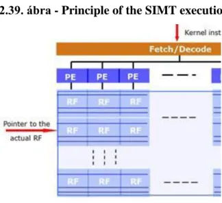
2.39. Principle of the SIMT execution ... 42
2.40. Principle of the SIMT execution ... 42
2.41. Contrasting key features of SIMD and SIMT execution ... 43
2.42. Key abstractions of the execution model ... 43
2.43. Segmenting the domain of execution to work-groups ... 44
2.44. ... 44
2.45. ... 45
2.46. ... 45
2.47. ... 46
2.48. ... 46
2.49. Key abstractions of the execution model ... 47
2.50. ... 48
2.51. ... 48
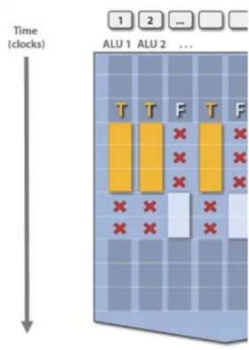
2.52. Execution of branches-1 [26] ... 49
2.53. Execution of branches-2 [26] ... 49
2.54. Resuming instruction stream processing after executing a branch [26] ... 50
2.55. Key abstractions of the execution model ... 50
2.56. ... 51
2.57. ... 52
2.58. ... 52
2.59. ... 53
2.60. ... 53
2.61. ... 54
2.62. ... 55
2.63. ... 56
2.64. ... 56
2.65. ... 56
2.66. ... 57
2.67. ... 58
3.1. Basic implementation alternatives of the SIMT execution ... 59
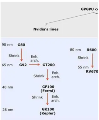
3.2. Overview of Nvidia’s and AMD/ATI’s GPGPU lines ... 59
3.3. Overview of GPGPU cores and cards and their basic software support (1) ... 60
3.4. Overview of GPGPU cores and cards and their basic software support (2) ... 60
3.5. Overview of GPGPU cores and cards and their basic software support (3) ... 61
3.6. Main features of Nvidia’s dual-GPU graphics cards [33], [34] ... 62
3.7. Main features of AMD’s/ATI’s dual-GPU graphics cards [35] ... 62
3.8. ... 62
3.9. Main features of Nvidia’s pre-Fermi graphics cards [33] ... 63
3.10. Interpretation of the MAD (Multiply-Add) operation [51] ... 64
3.11. ... 64
3.12. Main features of Nvidia’s Fermi-based graphics cards [33] ... 65
3.13. Main features of Nvidia’s Kepler-based graphics cards [33] ... 66
3.14. ... 67
3.15. ... 68
3.16. ... 69
3.17. ... 69
3.18. ... 70
3.19. ... 70
3.20. Main features of AMD/ATI’s early graphics cards-1 [35] ... 71
3.21. Main features of AMD/ATI’s early graphics cards-2 [35] ... 72
3.22. Main features of AMD’s Southern Islands series graphics cards [35] ... 72
3.23. Main features of AMD’s Northern Islands series graphics cards [35] ... 73
3.24. Main features of AMD’s Southern Islands series (GCN) graphics cards [35] ... 74
3.25. Main features of AMD’s Sea Islands series graphics cards [45] ... 74
3.26. ATI HD 5870 (RV870 based) [43] ... 75
3.27. ATI HD 5970: 2 x ATI HD 5870 with slightly reduced memory clock ... 76
3.28. ATI HD 5970: 2 x ATI HD 5870 with slightly reduced memory clock ... 76
3.29. AMD HD 6990: 2 x ATI HD 6970 with slightly reduced memory and shader clock ... 77
3.30. AMD HD 7970 ... 77
3.31. Summer 2012 GPU Pricing Comparison ... 78
4.1. Overview of GPGPU cores and cards and their basic software support (2) ... 80
4.2. ... 80
4.3. ... 81
4.4. ... 82
4.5. ... 83
4.6. ... 85
4.7. ... 85
4.8. ... 87
4.9. ... 88
4.10. ... 88
4.11. ... 88
4.12. ... 89
4.13. Fermi’s system architecture [52] ... 89
4.14. ... 90
4.15. ... 91
4.16. ... 92
4.17. ... 92
4.18. ... 93
4.19. ... 94
4.20. ... 95
4.21. A single ALU [57] ... 95
4.22. Contrasting the Multiply-Add (MAD) and the Fused-Multiply-Add (FMA) operations [51] 96
4.23. Hierarchy of threads [58] ... 96
4.24. ... 97
4.25. ... 97
4.26. ... 99
4.27. ... 99
4.28. ... 101
4.29. The Bulldozer core [60] ... 102
4.30. The Fermi core [52] ... 102
4.31. The Fermi core [52] ... 104
4.32. The Fermi core [52] ... 105
4.33. ... 106
4.34. ... 107
4.35. Warp scheduling in the G80 [59] ... 108
4.36. Warp scheduling in the G80 [59] ... 109
4.37. Warp scheduling in the G80 [59] ... 110
4.38. The Fermi core [52] ... 111
4.39. The Fermi core [52] ... 113
4.40. Contrasting the overall structures of the GF104 and the GF100 [62] ... 114
4.41. ... 115
4.42. ... 116
4.43. ... 116
4.44. ... 118
4.45. ... 119
4.46. ... 119
4.47. ... 120
4.48. ... 121
4.49. ... 122
4.50. ... 123
4.51. ... 123
5.1. Overview of GPGPU cores and cards and their basic software support (3) ... 125
5.2. ... 125
5.3. Block dagram of the GK104 Kepler core ... 125
5.4. Block diagram of the GK110 Kepler core ... 126
5.5. ... 126
5.6. Principle of dynamic parallelism in Kepler GPUs ... 128
5.7. Serial and Concurrent Kernel execution models of Fermi and pre-Fermi devices [25], [18] .. 128
5.8. Serial and Concurrent Kernel execution models of Fermi and pre-Fermi devices [25], [18] . 129 5.9. Using a single hardware work queue to schedule multiple streams of kernels [70] ... 129
5.10. Fermi’s model of concurrent execution [70] ... 130
5.11. Principle of the Hyper-Q scheduling model [70] ... 131
5.12. Principle of Hyper-Q [70] ... 132
5.13. Kepler’s Hyper-Q scheduling mechanism used to issue simultaneous MPI tasks compared to the
MPI task issue mechanism of Fermi [73] ... 133
5.14. Contrasting the scheduling subsystems of the Fermi and Kepler architectures [70] ... 134
5.15. The GPU Direct feature of Kepler [70] ... 134
5.16. View of the Titan (Cray XK7) supercomputer [75] ... 135
5.17. Core clock frequency vs shader frequency in Nvidia’s major GPU families ... 136
5.18. Available execution resources in a Kepler SMX vs. a Fermi SM ... 137
5.19. Core clock frequency vs shader frequency in Nvidia’s major GPU families ... 137
5.20. ... 137
5.21. Main features of Nvidia’s and AMD’s GPU cards [77] ... 138
5.22. Comparing the power efficiency of the Fermi and Kepler designs [76] ... 138
5.23. Block diagram of Fermi’s hardware dependency checking [76] ... 139
5.24. Block diagram of Kepler’s hardware dependency checking [76] ... 139
5.25. ... 139
5.26. ... 139
5.27. ... 140
5.28. Key device features bound to the compute capability versions [32] ... 140
5.29. Kepler’s cache architecture [70] ... 141
5.30. ... 142
5.31. Block dagram of the GK104 Kepler core ... 143
5.32. ... 143
5.33. ... 144
5.34. Main features of Nvidia’s Kepler-based GTX 680 GPGPU card [33] ... 145
5.35. ... 145
5.36. ... 147
5.37. ... 147
5.38. Block diagram of the GK110 Kepler core ... 148
5.39. ... 149
5.40. ... 149
5.41. ... 150
5.42. ... 151
5.43. ... 153
5.44. ... 153
5.45. ... 154
5.46. ... 154
6.1. ... 155
6.2. ... 156
6.3. AMD’s view of the evolution to heterogeneous computing [84] ... 156
6.4. ... 158
6.5. The compilation phase ... 158
6.6. The runtime phase ... 159
6.7. Classical retargetable tree-phase compiler design [89] ... 160
6.8. ... 161
6.9. ... 161
6.10. ... 162
7.1. ... 163
7.2. Overview of GPGPU cores and cards and their basic software support (3) ... 164
7.3. ... 164
7.4. Evolution of the microarchitecture of ATI’s (acquired by AMD in 2006) and AMD’s GPUs [95] 165 7.5. Block diagram of a VLIW5 ALU [17] ... 165
7.6. ... 166
7.7. Block diagram of a VLIW4 ALU (introduced in the Northern Island line (HD6900 line)) [17] 166 7.8. Simplified block diagram of a 16-wide SIMD unit (based on [95]) ... 167
7.9. ... 167
7.10. ... 168
7.11. Main steps of the evolution of AMD’s VLIW-based shader ALUs ... 169
7.12. The vertex shader pipeline in ATI’s first GPU supporting DX 9.0 (The R300 core) (2002) [102] 170 7.13. Main steps of the evolution of AMD’s VLIW-based shader ALUs ... 170
7.14. Main steps of the evolution of AMD’s VLIW-based shader ALUs ... 171
7.15. Block diagram of the VLIW4 ALU introduced in the Northern Island line (HD6900 line) [17] 172 7.16. ... 172
7.17. ... 175
7.18. ... 176
7.19. ... 176
7.20. ... 177
7.21. Overview of GPGPU cores and cards and their basic software support (3) ... 178
7.22. Subfamilies of the "Southern Islands" Family [107] ... 179
7.23. ... 180
7.24. Overview of GPGPU cores and cards and their basic software support (3) ... 180
7.25. ... 181
7.26. Block diagram of the HD 5950 (Tahiti Pro) [109] ... 181
7.27. ... 182
7.28. ... 182
7.29. Simplified block diagram of a 16-wide SIMD unit (based on [95]) ... 183
7.30. ... 184
7.31. ... 185
7.32. ... 185
7.33. The interpretation of an N-Dimensional Range [12] ... 186
7.34. The interpretation of a work-item (Based on [12]) ... 187
7.35. The interpretation of workgroups [12] ... 188
7.36. The interpretation wavefronts [12] ... 189
7.37. Block diagram of a Southern Island Series processor [110] ... 190
7.38. Block diagram of a CU [110] ... 191
7.39. ... 192
7.40. ... 192
7.41. ... 193
7.42. ... 194
7.43. ... 195
8.1. ... 197
8.2. ... 197
8.3. Overview AMD’s Southern Islands and Sea Islands families of GPGPU cores and cards .... 198
9.1. ... 199
9.2. ... 200
9.3. Intel’s Package-on-Package memory stacking used in the Clover Trail tablet platform [116] 200 9.4. AMD’s 2013 notebook graphics roadmap [117] ... 201
9.5. AMD’s 2013 desktop graphics roadmap [117] ... 201
9.6. ... 201
9.7. ... 202
9.8. Overview of Intel’s Xeon Phi line (previously designated as the MIC line) ... 202
9.9. ... 203
9.10. ... 204
9.11. Main features of Intel’s Xeon Phi line [122], [123] ... 204
9.12. ... 205
9.13. The microarchitecture of Knights Corner [120] ... 206
9.14. ... 206
9.15. ... 206
9.16. ... 207
9.17. ... 207
9.18. ... 208
9.19. ... 209
9.20. ... 209
9.21. ... 210
9.22. ... 210
9.23. ... 211
9.24. ... 211
9.25. ... 212
9.26. ... 213
9.27. ... 214
1.1. [11] ... 228
1.2. ... 228
1.3. [3] ... 230
1.4. [5] ... 231
1.5. [3] ... 232
1.6. [7] ... 233
2.1. ... 234
2.2. [5] ... 235
2.3. [5] ... 237
2.4. [2] ... 238
2.5. ... 242
2.6. ... 242
2.7. [5] ... 243
2.8. [5] ... 245
2.9. ... 246
2.10. ... 247
2.11. ... 247
2.12. ... 248
2.13. [5] ... 248
2.14. ... 249
2.15. [5] ... 249
2.16. ... 250
2.17. [5] ... 250
2.18. [5] ... 251
2.19. ... 252
2.20. ... 253
2.21. [5] ... 253
2.22. ... 254
2.23. [5] ... 254
2.24. ... 255
2.25. [5] ... 255
2.26. [5] ... 256
2.27. ... 258
2.28. ... 258
2.29. ... 259
2.30. ... 259
2.31. ... 259
2.32. [5] ... 260
2.33. ... 261
2.34. [5] ... 263
2.35. ... 266
2.36. ... 267
2.37. ... 267
2.38. ... 268
2.39. ... 268
3.1. ... 270
3.2. ... 271
3.3. ... 272
3.4. ... 272
3.5. ... 275
3.6. ... 276
3.7. [12] ... 280
3.8. ... 280
3.9. ... 280
3.10. ... 281
3.11. ... 281
3.12. ... 282
3.13. ... 282
3.14. [12] ... 284
3.15. [12] ... 284
3.16. ... 285
3.17. ... 285
3.18. ... 285
3.19. ... 286
3.20. ... 286
3.21. ... 287
3.22. ... 288
3.23. [9] ... 289
3.24. ... 290
3.25. [10] ... 290
3.26. ... 291
3.27. ... 291
3.28. ... 292
3.29. ... 292
3.30. ... 292
3.31. ... 292
3.32. ... 292
3.33. ... 292
3.34. ... 293
3.35. ... 293
4.1. ... 296
4.2. ... 296
4.3. ... 297
4.4. ... 297
4.5. ... 297
4.6. ... 297
4.7. ... 298
4.8. ... 298
4.9. ... 298
4.10. ... 300
4.11. ... 301
4.12. ... 301
4.13. ... 301
4.14. ... 301
4.15. ... 303
4.16. ... 303
4.17. ... 304
4.18. ... 305
4.19. ... 306
4.20. ... 307
4.21. ... 308
4.22. ... 310
4.23. ... 311
4.24. ... 311
4.25. ... 312
4.26. ... 313
4.27. ... 314
4.28. ... 314
4.29. ... 314
4.30. ... 315
4.31. ... 318
4.32. ... 319
4.33. ... 319
4.34. ... 320
4.35. ... 322
4.36. ... 323
4.37. ... 324
4.38. ... 324
4.39. ... 325
4.40. ... 325
4.41. ... 327 5.1. ... 329 6.1. ... 334 6.2. ... 335 6.3. ... 335 6.4. ... 336 6.5. ... 337 6.6. ... 337
I. rész - GPGPUs
Tartalom
Aim ... ix 1. Introduction to GPGPUs ... 10 1. Representation of objects by triangles ... 10 1.1. Main types of shaders in GPUs ... 11 2. Convergence of important features of the vertex and pixel shader models ... 12 3. Peak FP32/FP64 performance of Nvidia’s GPUs vs Intel’ P4 and Core2 processors [7] .. 14 4. Peak FP32 performance of AMD’s GPUs [8] ... 15 5. Evolution of the FP-32 performance of GPUs [9] ... 16 6. Evolution of the bandwidth of Nvidia’s GPU’s vs Intel’s P4 and Core2 processors [7] .... 16 7. Comparing main features of CPUs and GPUs [12] ... 17 2. The virtual machine concept of GPGPU computing ... 19 1. Introduction to the virtual machine concept of GPGPU computing ... 19 1.1. The virtual machine concept as used for GPGPUs ... 19 1.2. Benefits of the portability of the pseudo assembly code ... 19 1.3. The process of developing applications-1 ... 19 1.4. The process of executing applicatons-2 ... 20 1.5. Formulation of application programs at different levels of abstraction ... 20 2. Introduction to a GPGPU-based massively data parallel computational model ... 21 2.1. Specification of GPGPUs at different levels of abstraction ... 21 2.2. Specification of the GPGPU virtual machine ... 22 2.3. The GPGPU-based massively data parallel computational model ... 22 2.4. Emergence of GPGPU-based massively data parallel computational models ... 22 2.5. The choice of the computational model presented ... 23 2.6. The choice of the terminology used ... 23
2.6.1. Designation of the GPGPU-based massively data parallel computational model as the SIMT (Single instruction Multiple Threads) model of computation ... 23 2.6.2. Designation of the terms related to GPGPU-based massively data parallel computational model ... 23 3. Introduction to the SIMT computational model ... 24 3.1. Main components of the SIMT computational models ... 24 3.2. The model of the compute workload ... 24 3.2.1. The thread model ... 25 3.2.2. The kernel concept ... 29 3.3. The model of the platform ... 31 3.3.1. The model of computational resources ... 31 3.3.2. The memory mode ... 35 3.4. The execution model ... 39 3.4.1. The concept of SIMT execution ... 39 3.4.2. The concept of assigning work to the PEs ... 43 3.4.3. The concept of data sharing ... 47 3.4.4. The concept of data dependent flow control ... 48 3.4.5. The concept of synchronization ... 50 4. The Pseudo ISA of GPGPU computing ... 51 4.1. Discussion of pseudo ISAs ... 52 4.2. Case example: The pseudo ISA of Nvidia’s PTX virtual machine ... 52 4.3. Case example: The pseudo ISA of Nvidia’s PTX virtual machine ... 53 4.4. Nvidia’s compute capability concept [31], [1] ... 54 4.5. a) Evolution of the functional features, called compute capabilities in subsequent versions of Nvidia’s pseudo ISA (PTX) [32] ... 55 4.6. b) Evolution of the device parameters bound to subsequent compute capability versions of Nvidia’s PTX [32] ... 55 4.7. c) Architecture specifications bound to compute capability versions of Nvidia’s PTX [32]
... 56 4.8. d) Throughput of native arithmetic instructions in subsequent compute capability versions of Nvidia’s PTX (operations per clock cycle/SM) [7] ... 56
4.9. PTX ISA Versions generated by subsequent releases of CUDA SDKs and supported compute capability versions (sm[xx]) (designated as Supported Targets in the Table) [20]
57
4.10. Compute capability versions supported by Nvidia’s GPGPU cores and cards [32] 58 4.11. Forward portability of PTX code [31] ... 58 4.12. Compatibility rules of object files (CUBIN files) compiled to a particular GPGPU compute capability version [31] ... 58 3. Overview of GPGPU cores and cards ... 59 1. General overview ... 59 1.1. GPGPU cores ... 59 1.2. Main features of Nvidia’s dual-GPU graphics cards ... 62 1.3. Main features of AMD’s/ATI’s dual-GPU graphics cards ... 62 1.4. Remarks on AMD-based graphics cards [36], [37] ... 62 2. Overview of the main features of Nvidia’s graphics cores and cards ... 63 2.1. Main features of Nvidia’s graphics cores and cards ... 63 2.1.1. Structure of an SM of the G80 architecture ... 64 2.1.2. Positioning Nvidia’s GPGPU cards in their entire product portfolio [41] 67 2.2. Examples for Nvidia’s graphics cards ... 68 2.2.1. Nvidia GeForce GTX 480 (GF 100 based) [42] ... 68 2.2.2. A pair of Nvidia’s GeForce GTX 480 cards [42] (GF100 based) ... 68 2.2.3. Nvidia’s GeForce GTX 480 and 580 cards [44] ... 69 2.2.4. Nvidia’s GTX 680 card [80] (GK104 based) ... 70 2.2.5. Nvidia’s GTX Titan card [81] (GK110 based) ... 70 3. Overview of the main features of AMD’s graphics cores and cards ... 71 3.1. Main features of AMD’s graphics cores and cards ... 71 3.2. Examples for AMD’s graphics cards ... 75 3.2.1. ATI HD 5970 (actually RV870 based) [46] ... 76 3.2.2. ATI HD 5970 (RV870 based) [47] ... 76 3.2.3. AMD HD 6990 (Cayman based) [48] ... 77 3.2.4. AMD Radeon HD 7970 (Tahiti XT, Southern Islands based) - First GCN implementation [49] ... 77 3.2.5. Prices of GPGPUs as of Summer 2012 [50] ... 78 4. Nvidia’s Fermi family of graphics cores and cards ... 80 1. Overview of the Fermi family ... 80 1.1. Major sub-families of Fermi ... 81 2. Key innovations of Fermi’s PTX 2.0 ... 81 2.1. Overview of PTX 2.0 ... 81 2.2. Key innovations of PTX 2.0 pseudo ISA ... 82
2.2.1. a) Unified address space for all variables and pointers with a single set of load/store instructions-1 [11] ... 82 2.2.2. a) Unified address space for all variables and pointers with a single set of load/store instructions-2 [11] ... 82 2.2.3. b) 64-bit addressing capability ... 83 2.2.4. c) New instructions to support OpenCL and DirectCompute APIs ... 83 2.2.5. d) Full support of predication [51] ... 83 2.2.6. e) Full IEEE 754-3008 support for 32-bit and 64-bit FP precision ... 84 2.2.7. Supporting program development for the Fermi line of GPGPUs [11] ... 84 3. Major innovations and enhancements of Fermi’s microarchitecture ... 84 3.1. Major innovations ... 84 3.2. Major enhancements ... 84 3.3. Major architectural innovations of Fermi ... 85 3.3.1. a) Concurrent kernel execution [52], [18] ... 85 3.3.2. b) True two level cache hierarchy [11] ... 85 3.3.3. c) Configurable shared memory/L1 cache per SM [11] ... 86 3.3.4. d) ECC support [11] ... 87 3.4. Major architectural enhancements of Fermi ... 87 3.4.1. a) Vastly increased FP64 performance ... 88 3.5. Throughput of arithmetic operations per clock cycle per SM [13] ... 88 3.5.1. b) Greatly reduced context switching times [11] ... 88 3.5.2. c) 10-20 times faster atomic memory operations [11] ... 89
4. Microarchitecture of Fermi GF100 ... 89 4.1. Overall structure of Fermi GF100 [18], [11] ... 89 4.2. High level microarchitecture of Fermi GT100 ... 89 4.3. Evolution of the high level microachitecture of Nvidia’s GPGPUs [52] ... 90 4.4. Layout of a Cuda GF100 SM [19] ... 91 4.5. Evolution of the cores (SMs) in Nvidia’s GPGPUs -1 ... 91 4.6. Further evolution of the SMs in Nvidia’s GPGPUs -2 ... 93 4.7. Structure and operation of the Fermi GF100 GPGPU ... 94 4.7.1. Layout of a Cuda GF100 SM [19] ... 94 4.7.2. A single ALU (“CUDA core”) ... 95 4.8. Principle of the SIMT execution in case of serial kernel execution ... 96 4.9. Principle of operation of a Fermi GF100 GPGPU ... 96 4.10. Subtasks of work scheduling ... 96 4.11. Scheduling kernels to SMs [25], [18] ... 97 4.12. Scheduling thread blocks associated with the same kernel to the SMs ... 97 4.13. The notion and main features of thread blocks in CUDA [53] ... 98 4.14. Segmenting thread blocks into warps [59] ... 99 4.15. Scheduling warps for execution in SMs ... 100 4.16. Assumed principle of operation-1 ... 102 4.17. Assumed principle of operation-2 ... 103 4.18. Assumed principle of operation-3 ... 104 4.19. Example: Throughput of arithmetic operations per clock cycle per SM [13] .... 106 4.20. Scheduling policy of warps in an SM of Fermi GF100-1 ... 107 4.21. Scheduling policy of warps in an SM of Fermi GT100-2 ... 108 4.22. Scheduling policy of warps in an SM of the G80 indicating coarse grain warp scheduling ... 109 4.23. Scheduling policy of warps in an SM of the G80 indicating fine grain warp scheduling 109
4.24. Estimation of the peak performance of the Fermi GF100 -1 ... 110 4.25. Estimation of the peak performance of the Fermi GF100 -2 ... 112 5. Microarchitecture of Fermi GF104 ... 114 5.1. Available execution resources per SM in the GF104 vs the GF100 ... 115 5.2. Throughput of arithmetic operations per clock cycle per SM in the GF104/114 [13] 116 5.3. Warp issue in the Fermi GF104 ... 116 5.4. Peak computational performance data for the Fermi GF104 based GTX 460 card 117 6. Microarchitecture of Fermi GF110 ... 118
6.1. Overall structure of the Fermi Gf110 core [65] ... 118 6.2. Block diagrams of the cores (SM units) of the four sub-families of Fermi [66] .. 119 6.3. Throughput of arithmetic operations per clock cycle per SM in the GF104/114 [13] 120 7. Microarchitecture of Fermi GF114 ... 121
7.1. Overall structure of the Fermi GF114 core in the GTX 560 card [67] ... 121 7.2. Microarchitecture of Fermi GF114 ... 122 7.3. Block diagrams of the cores (SM units) of the four sub-families of Fermi [66] .. 123 7.4. Throughput of arithmetic operations per clock cycle per SM in the GF104/114 [13] 123 5. Nvidia’s Kepler family of graphics cores and cards ... 125
1. Overview of Nvidia’s Kepler family ... 125 1.1. Sub-families of Kepler ... 125 1.2. The GK104 Kepler core [76] ... 125 1.3. The GK110 Kepler core [70] ... 126 1.4. Main features of Nvidia’s Kepler GK104 and GK110 cores [70] ... 126 2. Key innovations of Kepler’s PTX 3.x ... 127 3. Major innovations of Kepler’s microarchitecture ... 127 3.1. a) Dynamic parallelism [70] ... 127 3.1.1. Principle of dynamic parallelism in Kepler GPUs ... 128 3.1.2. Benefits of dynamic parallelism [70] ... 128 3.2. b) The Hyper-Q scheduling mechanism ... 128 3.2.1. Speed up potential of the Hyper-Q scheduling mechanism ... 133 3.3. c) Grid Management Unit ... 134 3.4. d) The GPU Direct feature ... 134 3.5. Major enhancements of Kepler’s microarchitecture ... 135
3.5.1. a) Setting down the operating frequency of the execution units (shader clock frequency) to the core frequency-1 ... 136 3.5.2. a) Setting down the operating frequency of the execution units (shader clock frequency) to the core frequency-2 ... 136 3.5.3. a) Setting down the operating frequency of the execution units (shader clock frequency) to the core frequency-3 ... 136 3.5.4. a) Setting down the operating frequency of the execution units (shader clock frequency) to the core frequency-4 ... 137 3.5.5. Comparing the silicon area needed and power consumption of the design approaches used to implement Fermi’s and Kepler’s execution units [76] ... 137 3.5.6. b) Simplifying hardware dependency checks by introducing compiler hints 139 3.5.7. c) Introducing quad warp schedulers per SMX ... 139 3.5.8. Available execution resources in a Kepler SMX vs. a Fermi SM ... 139 3.5.9. d) Quadrupling the number of registers that are accessible per thread .... 140 3.5.10. Consequence of quadrupling the number of registers that can be accessed per thread in the cores of Kepler ... 141 3.5.11. e) Introduction of a 48 KB Read-Only data cache for general use ... 141 3.5.12. f) Doubled L2 cache size and bandwidth vs. Fermi ... 142 4. Nvidia’s GK104 Kepler core and related graphics cards ... 142 4.1. Sub-families of Kepler ... 142 4.2. The GK104 Kepler core [76] ... 143 4.3. Die photo of Nvidia’s Kepler GK104 core [78] ... 143 4.4. Block diagram of an SMX of the Kepler GK104 core [76] ... 144 4.5. Peak FP32 and FP34 performance of the GK104 based GeForce GTX 680 graphics card 145
4.5.1. a) Peak FP32 performance of the GK104 based GeForce GTX 680 graphics card- 1 ... 145 4.5.2. a) Peak FP32 performance of the GK104 based GeForce GTX 680 graphics card- 2 [70] ... 145 4.5.3. a) Peak FP32 performance of the GK104 based GeForce GTX 680 graphics card- 3 ... 146 4.5.4. b) Peak FP64 performance of the GK104 based GeForce GTX 680 graphics card- 1 ... 146 4.5.5. b) Peak FP64 performance of the GK104 based GeForce GTX 680 graphics card- 2 [70] ... 147 4.5.6. b) Peak FP64 performance of the GK104 based GeForce GTX 680 graphics card- 3 ... 147 5. Nvidia’s GK110 Kepler core and related graphics cards ... 147 5.1. Sub-families of Kepler ... 147 5.2. The GK110 core ... 148 5.3. The GK110 Kepler core [70] ... 148 5.3.1. Die photo of Nvidia’s Kepler GK110 core [70] ... 148 5.3.2. Die layout of Nvidia’s Kepler GK110 core [79] ... 149 5.3.3. Comparison of the die sizes of Nvidia’s GK110 and GK104 Kepler cores [79]
150
5.3.4. Block diagram of an SMX of the Kepler GK110 core [70] ... 151 5.3.5. a) Peak FP32 performance of the GK110 based GeForce GTX Titan graphics card ... 152 5.3.6. b) Peak FP64 performance of the GK110 based GeForce GTX Titan graphics card ... 152 6. Evolution of Nvidia’s microarchitectures ... 152 6.1. a) Evolution of FP32 warp issue efficiency in Nvidia’s pre-Fermi GPGPUs ... 153 6.2. b) Evolution of FP32 warp issue efficiency in Nvidia’s Fermi and Kepler GPGPUs 153 6.3. c) FP64 performance increase in Nvidia’s pre-Fermi GPGPUs ... 153 6.4. d) FP64 performance increase in Nvidia’s Tesla and GPGPUs ... 154 6. AMD’s Heterogeneous Systems Architecture concept ... 155 1. Introduction to the HSA concept ... 155 1.1. First public introduction of the HSA concept (6/2011) [84], [85] ... 155 1.2. Aims of the Heterogeneous Systems Architecture (HSA) concept ... 156
1.2.1. AMD’s view of the evolution of single core, multi-core and application performance (6/2011) [84] ... 156 1.2.2. AMD’s view of the evolution path to heterogeneous computing (6/2011) [84]
156
2. The vision of the HSA concept ... 156 2.1. a) The memory model of HSA [87] ... 157 2.2. b) User-level command queuing [87] ... 157 2.3. d) Model of processing applications [88] ... 158 2.4. Principle of processing applications in HSA [87] ... 158 2.5. The runtime phase [87] ... 159 2.6. Heterogeneous System Architecture Foundation (HSAF) ... 161 2.7. AMD’s roadmap for the implementation of HSA [90] ... 161 2.8. AMD’s roadmap for the implementation of HSA - a more detailed view [85] ... 162 7. AMD’s Southern Islands family of graphics cores and cards ... 163 1. Overview of AMD’s Southern Island family ... 163
1.1. AMD’s roadmap for the implementation of HSA (Financial Analyst Day 2/2012) [90]
163
1.2. AMD’s new GPU microarchitecture: the Graphics Core Next (GCN) ... 163 1.3. Announcement and implementation of AMD’s GCN ... 164 1.4. AMD’s roadmap indicating the introduction of GCN along with the Southern Islands line (2/2012) [94] ... 164 2. Major innovations of the Southern Islands microarchitecture ... 164
2.1. AMD’s move from the VLIW4-based GPU design to the SIMD-based GPU design 164 2.1.1. Main steps of the evolution of the microarchitecture of ATI’s (acquired by AMD in 2006) and AMD’s GPU’s [95] ... 165 2.1.2. Principle of using VLIW-based ALUs in GPUs ... 165 2.1.3. VLIW-based ALUs ... 166 2.1.4. Example for encoding wavefront queues in form of VLIW4 instructions [96]
166
2.1.5. Scheduling the wavefronts given previously while assuming VLIW4 encoding [96] ... 167 2.1.6. Graphics processing and VLIW-based ALUs ... 168 2.1.7. AMD’s motivation for using VLIW-based ALUs in their previous GPU’s 168 2.1.8. Number of execution units (EUs) in Nvidia’s and AMD’s GPUs ... 168 2.1.9. AMD’s motivation for using VLIW5-based ALUs in their first GPU’s [97] 169 2.1.10. AMD’s VLIW5 design ... 169 2.1.11. Replacing the original VLIW5 design by the Enhanced VLIW5 design 170 2.1.12. Replacing the Enhanced VLIW5 design by the VLIW4 design-1 ... 171 2.1.13. Replacing the Enhanced VLIW5 design with the VLIW4 design-2 ... 171 2.1.14. Contrasting the main features of AMD’s Enhanced VLIW5 and VLIW4 designs [17] ... 172 2.1.15. Shift to numeric computing and AMD’s move to the GCN architecture 174 2.1.16. Replacing the VLIW4-based design by SIMD-based design in AMD’s GCN architecture [91] ... 175 2.2. AMD ZeroCore technology [49] ... 175
2.2.1. Achieved reduction of power consumption in long idle periods in AMD’s GPUs due to using the AMD ZeroCore Power Technology [104] ... 176 2.2.2. The AMD PowerTune technology ... 176 2.2.3. The PowerTune technology as introduced in the Northern Island line (HD 6900/Cayman), 12/2010) [106] ... 176 2.2.4. Benefit of using the PowerTune technology [105] ... 177 3. AMD’s Southern Islands card family ... 178 3.1. Overview of the Southern Islands family ... 178 3.1.1. Announcement and implementation of AMD’s GCN ... 178 3.1.2. Key features of the Southern Island Family ... 179 3.1.3. Subfamilies of the Southern Island Family-1 [107] ... 179 3.1.4. Comparison of the die sizes of AMD’s and Nvidia’s graphics cores [95] 180 3.1.5. Announcement and implementation of AMD’s GCN ... 180 3.2. Microarchitecture of the Tahiti XT core used in the Radeon HD7970 card ... 181 3.2.1. Overall architecture of the Tahiti XT core [95] ... 181
![1.12. ábra - Contrasting the utilization of the silicon area in CPUs and GPUs [10]](https://thumb-eu.123doks.com/thumbv2/9dokorg/1129370.80013/39.892.106.312.110.634/ábra-contrasting-utilization-silicon-area-cpus-gpus.webp)
![2.19. ábra - The model of computational resources [15]](https://thumb-eu.123doks.com/thumbv2/9dokorg/1129370.80013/54.892.105.430.673.1090/ábra-model-computational-resources.webp)
![2.31. ábra - Available data spaces in AMD’s IL vers. 2.0 [22]](https://thumb-eu.123doks.com/thumbv2/9dokorg/1129370.80013/60.892.106.395.91.480/ábra-available-data-spaces-in-amd-il-vers.webp)

![2.35. ábra - Scheduling wavefronts for hiding stalls due to device memory reads [24]](https://thumb-eu.123doks.com/thumbv2/9dokorg/1129370.80013/62.892.111.421.241.451/ábra-scheduling-wavefronts-hiding-stalls-device-memory-reads.webp)