algorithms on parallel computing platforms
Csaba Nemes
A thesis submitted for the degree of Doctor of Philosophy
Scientific adviser:
Zoltán Nagy, PhD Supervisor:
Péter Szolgay, DSc
Faculty of Information Technology And Bionics Péter Pázmány Catholic University
Budapest, 2014
Acknowledgements
First of all, I would like to thank my scientific advisor Zoltán Nagy and my consultant Prof. Péter Szolgay for guiding and supporting me over the years.
I am equally thankful to Örs Legeza and Gergely Barcza for teaching me quantum physics. Furthermore, I would like to give an extra special thank to Gergely Barcza for supporting me as a friend and as the godfather of my son.
I am grateful to Prof. Tamás Roska, Prof. Árpád Csurgay and Judit Nyékyné Gaizler, PhD for giving me encouragement and the opportunity to carry out my research at the university.
Conversations and lunches with Balázs Varga and Ádám Balogh are highly appreciated. Realistic thoughts from my ex-colleague and friend Tamás Fülöp always helped me to accurately determine my position even without a GPS. The cooperation of my closest colleagues András Kiss, Miklós Ruszinkó, Árpád Csík, László Füredi, Antal Hiba and Endre László is greatly acknowledged.
Most importantly, I am thankful to my family. I wish to thank my wife Fruzsi and son Zente for their loving care and tolerating my frequent ab- sence. Finally, I am lucky to have my parents, grandparents, and one great grandparent sponsoring my never-ending studies.
Contents
1 Introduction 1
2 Parallel architectures 5
2.1 Field Programmable Gate Arrays . . . 7
2.1.1 The general structure . . . 8
2.1.2 The common peripherals . . . 11
2.1.2.1 General purpose I/Os . . . 11
2.1.2.2 Transceiver I/Os . . . 12
2.1.3 Xilinx Virtex-6 SX475T FPGA . . . 13
2.2 Graphical Processing Units . . . 13
2.2.1 NVidia Kepler architecture . . . 15
2.2.1.1 The general structure . . . 15
2.2.1.2 CUDA programming . . . 16
2.2.1.3 NVidia K20 . . . 18
3 Solving Partial Differential Equations on FPGA 21 3.1 Computational Fluid Dynamics (CFD) . . . 21
3.1.1 Euler equations . . . 21
3.1.2 Finite volume method solution of Euler equations . . . 22
3.1.2.1 Structured mesh . . . 23
3.1.2.2 Unstructured mesh . . . 25
3.2 Data structures and memory access patterns . . . 27
3.3 Structure of the proposed processor . . . 29
3.4 Outline of the multi-processor architecture . . . 31
3.5 Analysis of the chosen design strategies . . . 32
v
4 Generating Arithmetic Units: Partitioning and Placement 35
4.1 Locally distributed control of arithmetic unit . . . 35
4.1.1 The proposed control unit . . . 35
4.1.2 Trade-off between speed and number of I/Os . . . 39
4.2 Partitioning problem . . . 40
4.2.1 Problem formulation . . . 40
4.3 Partitioning algorithms used in circuit design . . . 43
4.3.1 Move-based heuristics . . . 44
4.3.1.1 The Kernighan-Lin algorithm . . . 44
4.3.1.2 The Fiduccia-Mattheyses algorithm . . . 45
4.3.2 Spectral partitioning . . . 46
4.3.2.1 Spectral bipartitioning . . . 47
4.3.2.2 Spectral partitioning with multiple eigenvectors . . 48
4.3.3 Simulated annealing . . . 49
4.3.4 Software packages incorporating the multilevel paradigm . . . 50
4.3.4.1 Chaco . . . 51
4.3.4.2 hMetis . . . 52
4.4 Empirically validating the advantage of locally controlled arithmetic units . . . 53
4.4.1 The proposed greedy algorithm . . . 54
4.4.1.1 Preprocessing and layering . . . 56
4.4.1.2 Swap-based horizontal placement . . . 58
4.4.1.3 Greedy partitioning based on spatial information . . 59
4.4.2 The configuration of the hMetis program . . . 59
4.4.3 Comparison and evaluation . . . 61
4.5 Partitioning and placement together . . . 65
4.5.1 Properties of a good partition . . . 65
4.5.2 The proposed algorithm . . . 67
4.5.2.1 Preprocessing and Layering . . . 67
4.5.2.2 Floorplan with simulated annealing . . . 67
4.5.2.3 New representation for graph partitioning . . . 69
4.5.2.4 Partitioning . . . 72
4.5.2.5 Outline of the full algorithm . . . 74
4.5.3 Framework . . . 76
4.5.4 Results . . . 76
4.6 Summary . . . 77
5 Density Matrix Renormalization Group Algorithm 81 5.1 Previous implementations . . . 81
5.2 Investigated models . . . 82
5.2.1 Heisenberg model . . . 83
5.2.2 Hubbard model . . . 83
5.3 Symmetries to be exploited . . . 85
5.4 Algorithm . . . 86
5.4.1 LR strategy . . . 89
5.4.2 l-1-1-r strategy . . . 90
5.5 Parallelism and run-time analysis . . . 90
5.6 Limits of the FPGA implementation . . . 93
6 Hybrid GPU-CPU acceleration of the DMRG algorithm 95 6.1 Accelerating matrix-vector multiplications . . . 95
6.1.1 Architectural motivations . . . 97
6.1.2 gemv_trans() . . . 98
6.1.3 gemv() . . . 103
6.2 Accelerating projection operation . . . 103
6.2.1 Architectural motivations . . . 105
6.2.2 Scheduling strategies . . . 106
6.3 Implementation results . . . 110
6.4 Summary . . . 114
7 Summary of new scientific results 117 7.1 New Scientific Results . . . 117
7.2. Új tudomanyos eredmenyek (in Hungarian) . . . 121
7.2. Application of the Results . . . 125
References 134
Structure of the dissertation
Chapter 1introduces the motivation behind the scientific work presented in the disser- tation.
InChapter 2, frequently used parallel architectures are reviewed with emphasis on the FPGA and GPU architectures, which were used during my research.
InChapter 3, the numerical solution of partial differential equations on FPGAs is dis- cussed including two complex test cases, the description of the proposed architecture, and the analysis of the chosen design strategies. The chapter contains scientific results which belong to the research group I worked in, and provides the background infor- mation to the high-level design methodology (presented in the next chapter) which is my scientific contribution.
In Chapter 4, a new high-level design methodology is presented to design high-per- formance, locally controlled arithmetic units for FPGA. The chapter contains the sci- entific work related to my first thesis group.
Chapter 5provides the background information to the hybrid CPU-GPU acceleration of the density matrix renormalization group algorithm (presented in the next chapter).
It contains the description of the algorithm and the investigated models, which are part of the scientific literature, the run-time analysis of my CPU-only implementation, and my estimation of the performance of a possible FPGA acceleration.
InChapter 6the first hybrid CPU-GPU acceleration of the density matrix renormaliza- tion group algorithm is presented including a new scheduling for the matrix operations of the projection operation and a new CUDA kernel for the asymmetric transposed matrix-vector multiplication. The chapter contains the scientific work related to my second thesis group.
Finally, inChapter 7, the new scientific results of the dissertation are summarized, and the possible application areas are enumerated.
List of Figures
2.1 Schematic view of a simplified FPGA . . . 9
2.2 Schematic of a simplified logic cell . . . 9
2.3 A schematic block diagram of the Kepler GK110 chip . . . 17
3.1 A simulation of the airflow inside a scramjet engine . . . 23
3.2 Interface with the normal vector and the cells required in the computation 26 3.3 An unstructured mesh and the corresponding descriptors . . . 28
3.4 Block diagram of the proposed processor . . . 30
3.5 Outline of the proposed architecture . . . 32
4.1 Schematic of the control unit . . . 37
4.2 A partitioned data-flow graph and the corresponding cluster adjacency graph . . . 38
4.3 Operating frequency of the proposed control unit. . . 40
4.4 Placed instances of a locally controlled AU produced with a naive par- titioning technique . . . 55
4.5 A simple data-flow garph and its layered version . . . 57
4.6 The structured CFD graph partitioned by the proposed algorithm . . . 60
4.7 Placed instances of the locally controlled AU produced with the pro- posed partitioning . . . 62
4.8 A fragment of the first belt of Figure 4.9 is shown to demonstrate how inheritance works. . . 70
4.9 The partitioned data-flow graph of the unstructured CFD problem . . 74
4.10 Operating frequency and area requirements of the AU as the maximum number of I/O connections of a cluster is changing. . . 77
xi
5.1 Exploiting the projection symmetry in the Heisenberg model . . . 87
5.2 Exploiting the conservation of particle number in the spin-12 Hubbard model . . . 87
5.3 Heisenberg model: The run-time analysis of the algorithm . . . 91
5.4 Hubbard model: The run-time analysis of the algorithm . . . 91
6.1 The memory request of gemv_trans() in case of the Heisenberg model 96 6.2 GTX 570: Performance of the presentedgemv_trans()kernel . . . 98
6.3 K20, no shuffle operation in the kernel: Performance of the presented gemv_trans()kernel . . . 100
6.4 K20, shuffle operation enabled: Performance of the presentedgemv_- trans()kernel . . . 101
6.5 Similar to Figure 6.4 but for matrix height5e5. . . 102
6.6 Similar to Figures 6.4 and 6.5 but for matrix height1e6. . . 102
6.7 Performance of the gemv_normal() operation . . . 103
6.8 GPU memory footprints of the two strategies are compared in case of the Heisenberg model . . . 105
6.9 Interleaved operation records and the resulting parallel execution . . . 108
6.10 GTX 570, Heisenberg model: Performance of the two strategies is compared. . . 109
6.11 Similar to Figure 6.10 but on K20 architecture. . . 109
6.12 GTX 570, Heisenberg model: Performance results of the hybrid CPU- GPU acceleration of the projection operation. . . 111
6.13 Similar to Figure 6.12 but for the Hubbard model on GTX 570. . . 111
6.14 Similar to Figures 6.12 and 6.13 but for the Heisenberg model on K20. 112 6.15 Similar to Figures 6.12, 6.13 and 6.14 but for the Hubbard model on K20. . . 112
6.16 K20, Heisenberg model: Acceleration of different parts of the algo- rithm is compared form = 4096. . . 114
6.17 K20, Hubbard model: Acceleration of different parts of the algorithm is compared form= 4096. . . 115
xii
List of Tables
2.1 Virtex-6 FPGA Feature Summary . . . 14
2.2 NVIDIA Tesla product line and the GTX 570 GPU . . . 16
4.1 Implementation results of different partitioning strategies in case of the 32 bit structured CFD problem. . . 63
4.2 Comparing operating frequency of the 32 bit and the 64 bit AU in case of the structured CFD problem. . . 63
4.3 Partitioning and implementation results of the structured CFD graph. . 78
4.4 Partitioning and implementation results of the unstructured CFD graph. 79 5.1 Virtex-7 XC7VX1140T FPGA feature summary . . . 93
6.1 Runtime of the accelerated matrix-vector operations of the Davidson algorithm . . . 104
6.2 Total time of strategies is compared . . . 110
6.3 Heisenberg model: final timings compared . . . 113
6.4 Hubbard model: final timings compared . . . 113
6.5 Model comparison in case of Xeon E5 + K20. . . 113
xiii
List of Abbreviations
ASIC Application-specific Integrated Circuit AU Arithmetic Unit
BLAS Basic Linear Algebra Subprograms BRAM Block RAM
CFD Computational Fluid Dynamics CLB Configurable Logic Blocks
CMOS Complementary metal–oxide–semiconductor CNN Cellular Neural/Nonlinear Network
CNN-UM Cellular Neural/Nonlinear Network - Universal Machine CPU Central Processing Unit
CRS Compressed Row Storage CU Control Unit
CuBLAS CUDA BLAS
CUDA Compute Unified Device Architecture DDR3 Double Data Rate type three SDRAM DDR4 Double Data Rate type four SDRAM DMA Direct Memory Access
xv
DMRG Density Matrix Renormalization Group DSP Digital Signal Processing
EC Edge Coarsening FIFO First In, First Out
FIR Finite Impulse Response FM Fiduccia-Mattheyses algorithm FPGA Field Programmable Gate Array FPU Floating-point Unit
FVM Finite Volume Method
GDDR5 Graphics Double Data Rate type five SDRAM GPU Graphical Processing Unit
HC Hyperedge Coarsening I/O Input/Output
IDE Integrated Development Environment IP Intellectual Property
KL Kernighan-Lin algorithm LUT Look-up Table
MAC Media Access Control MACC Multiply Accumulate MADD Multiply Add
MHC Modified Hyperedge Coarsening MKL Math Kernel Library
MUX Multiplexer
NIC Network Interface Controller OpenCL Open Computing Language OpenMP Open Multi-Processing
PCI Peripheral Component Interconnect PCIe PCI Express
PDE Partial Differential Equation RAM Random-access Memory
RDMA Remote Direct Memory Access RTL Register-transfer-level
SA Simulated Annealing
SATA Serial Advanced Technology Attachment SDK Software Development Kit
SDRAM Synchronous Dynamic RAM SIMD Single Instruction Multiple Data SIMT Single Instruction Multiple Threads SM Streaming Multiprocessor
SMX Kepler Streaming Multiprocessor SoC System-on-Chip
SP2 Second-order Spectral Projection algorithm SRAM Static RAM
SRAM Static Random Access Memory STL Standard Template Library TPS Tensor Product States UCF User Constraint File
VHDL VHSIC Hardware Description Language
xviii
Chapter 1 Introduction
Computationally intensive simulations of physical phenomena are inevitable to solve engineering and scientific problems. Simulations are used to test product designs with- out fabrication or to predict properties of new physical or chemical systems. Computer engineering has long since been dealing with the acceleration of simulations to de- crease the development time of new products or to improve the resulting quality by expanding the design space. Since clock frequency of processors reached the phys- ical limits caused by power dissipation, processor designers are focusing on multi- and many-core architectures to keep up with the predictions of Moore’s law. The goal of high-performance computing is to answer how to exploit the computing potential of these novel parallel architectures, such as GPU (Graphical Processing Unit) and FPGA (Field Programmable Gate Array), to solve computationally intensive problems.
During my research I investigated the acceleration of two specific problems with the following questions in mind: What is the best architecture for the given application?
How can the implementation methodology be improved? What performance can be reached, and what are the implementation tradeoffs in terms of speed, power and area?
The first problem I investigated was the numerical solution of partial differential equations(PDEs) on FPGAs. Nagy et al. demonstrated that the FPGA implementation of the emulated digital CNN-UM (Cellular Neural Network - Universal Machine) can be generalized to efficiently simulate various types of conservation laws viafinite vol- ume method(FVM) discretization of the given PDE with the Euler explicit scheme [9].
The mathematical expression (numerical scheme) which has to be evaluated for each cell in each iteration can be represented with a synchronous data-flow graph. As the
1
goal is to design a high-performance pipelinedarithmetic unit(AU), which can oper- ate at high frequency, each mathematical operation, i.e., node of the graph, is imple- mented with a dedicatedfloating-point unit(FPU). On recent high-end FPGAs, several floating-point units can be realized, which can operate at high frequency, however, the global control signals connected to each floating-point unit slow down the operating frequency of the rest of the circuit.
My research goal was to develop a novel design methodology which constructs high-performance, locally controlled AUs from synchronous data-flow graphs. My questions were the following: How shall I partition the data-flow graph to obtain clus- ters which can be controlled efficiently? How to control the clusters and how to connect them to avoid synchronization problems? What is the price of the improved frequency in terms of speed, power and area? Finally, how to automate the generation process of the AUs to drastically decrease the development time of new numerical simulations?
The second problem I investigated was theDensity Matrix Renormalization Group (DMRG) algorithm [10]. The algorithm is a variational numerical approach, which has become one of the leading algorithms to study the low energy physics of strongly correlated systems exhibiting chain-like entanglement structure [11]. The algorithm was developed to balance the size of the effective Hilbert space and the accuracy of the simulation, and its runtime is dominated by the iterative diagonalization of the Hamilton operator. As the most time-consuming step of the algorithm, which is the projection operation of the diagonalization, can be expressed as a sequence of dense matrix operations, the DMRG is an appealing candidate to fully utilize the computing power residing in novel parallel architectures.
As the algorithm had not been accelerated on parallel architectures (to the best of my knowledge), my research goal was to investigate on which architecture the algorithm can be implemented most efficiently. My objective was to give a high- performance, parallel and flexible implementation on the selected architecture, which can deal with wide range of DMRG configurations.
In Chapter 2, modern parallel architectures are reviewed focusing on the architec- tures utilized in the dissertation: the FPGA and the GPU. In Chapter 3, an FPGA acceleration of the numerical solution of PDEs is presented including the numeri- cal formulas of a Computational Fluid Dynamics (CFD) problem and the proposed FPGA framework. In Chapter 4, the proposed design methodology for constructing
entific work related to my first thesis group. In Chapter 5, the DMRG algorithm is summarized including a run-time analysis of the CPU-only code and an estimation of the performance of a possible FPGA acceleration. In Chapter 6, a hybrid GPU-CPU DMRG code is described including the acceleration of the projection operation and some asymmetric matrix-vector operations of the diagonalization. This chapter con- tains the scientific work related to my second thesis group. Finally, the new scientific results of the dissertation are summarized in Chapter 7.
Chapter 2
Parallel architectures
Parallel architectures are being designed from the beginning of high performance com- puting, however, since clock frequency reached the physical limits, they have got into the primary focus of chip makers. At the current 20-30nm technology, several pro- cessing elements (cores) can be packed into one chip and the resulting parallel archi- tectures can be used to continue the performance improvement of the CMOS chips for some extra years. The demand for new parallel architectures raised several archi- tectural questions which was answered differently by chip designers. Architectural differences are also due to the different application areas that different chip makers may target. Unfortunately, there is a very serious barrier in the way of packaging many cores, that is, many transistors into a single chip: the power wall. As the power consumption of a single transistor cannot be decreased below a physical limit, it is a constant challenge for chip designers to pack more performance into a single chip by designing more power efficient cores. (One possible way to decrease the power con- sumption of a chip is to "turn off" the parts which are currently not used, however, in high-performance applications, where all the resources are continuously utilized, this cannot be exploited.)
Multicore processors can be grouped into traditional multicore processors, in which a couple of heavy weight processing cores are glued on a single chip and to non- traditional multicore processors, which represent all the other efforts to design novel parallel architectures. The first group contains the traditional desktop and mobile CPUs of Intel and AMD, while the second group includes parallel efforts, such as IBM Cyclops-64 [12], IBM Cell [13], GPUs of NVidia and AMD, FPGAs of Xilinx and
5
Altera, Intel Larrabee [14], Intel MIC [15], and Tilera Tile-Gx [16].
One of the main questions arising in the many-core architecture design is the ques- tion of memory hierarchies and caches. At the dawn of novel parallel architectures it was still an open question, how to supply program developers with expensive au- tomated caching in complex systems. IBM chose a user-managed memory hierarchy approach in its Cell and Cyclops-64 processors. Cell processor was originally designed for Sony PlayStation 3 in the first half of 2000s, and it was reused in the IBM Road- runner supercomputer which was the first computer breaking through the ”petaflop barrier”. Cyclops-64 processor was also developed during the first half of 2000s and was one of the first projects to pack dozens of cores into a single chip: it contained 80 cores reaching80GFlops performance. Despite the success they reached, the architec- tures have been discontinued in the second half of 2000s. One of the main bottlenecks of their widespread usage was that it was relatively hard to develop efficient programs on them (compared to rivals) due to the user-managed memory hierarchy.
Graphical processing units (GPUs) entered the competition of general purpose par- allel architectures in 2006, when NVidia introduced its first unified shader architecture.
The proposed architecture introduced an universal processing core (stream processor) instead of vertex and pixel shader processors. The NVidia Geforce 8800 processor (codename G80) consisted of 128 stream processors grouped into 8 blocks by 16 pro- cessors. Each stream processor was a very simple, but universal processing core which was capable of floating-point operations. From the aspect of memory hierarchy, they took a middle course by implementing both automated and non-automated caches.
Nowadays, GPUs have an important role in high-performance computing, and the evo- lution of the architecture has not stopped. To review some of the new features of the modern GPUs, the NVidia Kepler architecture is presented in Section 2.2.
The success of GPUs inspired Intel to design its own GPU chip called Larrabee.
The idea behind the new architecture was to combine the advantages of CPUs and GPUs. Larrabee was intended to use very simple, but x86 instruction set cores and au- tomated cache mechanism across all the cores. The architecture was planned to contain 32computing cores and to reach one TFlops performance in case of single precision.
Although the chip had some working copies, it was not commercially released, and the architecture was replaced by the Intel Many Integrated Core (MIC) architecture.
The Intel MIC architecture was debuted under the brand name Xeon Phi in 2012. Intel
processor through a PCI express bus. The coprocessors of Intel Xeon Phi 7100 family contain 61 x86 instruction set cores connected via a very high bandwidth, bidirectional ring interconnect. Each core contains a vector processing unit with 512-bit SIMD in- struction set, which can execute 32 single-precision or 16 double-precision floating point operations per cycle (assuming multiply-and-add operation). In contrast with the GPUs, all cache memories are fully coherent and implement the x86 memory or- der model. Each core is equipped with a 32 KB L1 instruction cache, a 32 KB L1 data cache, and a 512 KB unified L2 cache. In case of double precision, the theoretical peak performance of the coprocessor is1208GFlops, while the peak memory bandwidth is 352GB/s.
In 2007, Tilera Corporation entered the high-performance multiprocessor industry with a novel many-core processors topology, in which the cores are interconnected via a 2D non-blocking mesh, called iMesh, forming an on-chip network. The Tile-Gx72 chip contains 72 processing cores, each of which is a full-featured 64-bit processor with fully coherent L1 and L2 caches. The chip integrates four DDR3 memory con- trollers (up to 1TB memory with 60GB/s) and several I/O controllers (e.g. 8 10 Gb/s Ethernet, 6 PCI express ports), therefore, there is no need for a host CPU. The product targets the cloud computing industry by being 3-4 times more energy efficient than Intel’s x86 based servers [17].
The FPGA represents a broader class of architectures as it is an universal chip which can be programmed to realize different types of architectures. However, as it can realize high-performance and power efficient parallel architectures, which compete with the previously mentioned chips, it can also be regarded as a highly customizable parallel architecture.
In the following sections, the FPGA and the GPU, the two architectures which are used in the dissertation, are presented in more detail.
2.1 Field Programmable Gate Arrays
Field Programmable Gate Arrays (FPGAs), introduced by Xilinx Inc in 1985, are sil- icon devices that can be electrically programmed to realize wide range of digital cir- cuits. They were created to fill the gap between fixed-function Application Specific
Integrated Circuits (ASICs) and software programs. From development aspects, they are still between the two approaches and, sometimes, the only compromise for appli- cations. In one hand, the fabrication time of ASICs cannot be compared to FPGAs that can be configured in less than a second. On the other hand, the development of an FPGA design usually takes significantly more time than a software development process. The reverse can be observed in case of power consumption: ASICs have the lowest power consumption, while FPGAs have lower power consumption than com- mon CPUs running the software programs. The speed performance of an FPGA is typically 3-4 times smaller than an ASIC [18], and the maximal operating frequency of an FPGA is 5-6 times smaller than a high-end CPU. Comparing the overall perfor- mance of FPGA and CPU is problematic because their performance is task dependent and in specific computational domains the FPGA outperforms the CPU contrary to the slower operating frequency.
2.1.1 The general structure
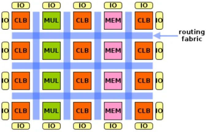
The schematic structure of an FPGA is illustrated in Figure 2.1. The main building blocks are the generic logic blocks, the dedicated blocks (e.g. memory or multiplier), the routing fabric, and the I/O blocks. During the implementation of a circuit, which is designed for FPGA, the blocks and the routing resources are electrically configured (programmed). The technology relies on electrically programmable switches which select the proper operation in the configurable blocks or the interconnection topology in the routing fabric. Currently, most FPGAs use static memory (SRAM) switches, but special FPGAs are also built with flash or anti-fuse technology. The main advantage of SRAM switches is the fast operation, however, they have to be reconfigured each time they are powered on.
In the beginning, FPGAs contained only very simple logic blocks, however, nowa- days, FPGAs contains complex logic blocks, which can be operated more efficiently in general. As a representative example, the logic block of Xilinx Virtex-6 FPGAs, also called Configurable Logic Block (CLB) is considered here. Each CLB contains two smaller logic cells, called slices. Every Virtex-6 slice contains four logic-function generators, also called look-up tables (LUTs), eight storage elements, wide-function multiplexers (MUX), and carry logic, which connects neighboring slices. To illustrate
Figure 2.1: Schematic view of a simplified FPGA containing only a few building blocks: con- figurable logic (CLB), multiplier (MUL), memory (RAM), and I/O blocks.
Figure 2.2: Schematic of a simplified logic cell
the concept, a simplified logic cell containing one 6-input LUT, two multiplexers, and one register is depicted in Figure 2.2. The 6-input LUT can be configured as a logic function, a 32-bit shift register, or a 64 bit memory. The storage element can act as a flip-flop or a latch. In case of Virtex-6, two types of slices are exist: SLICEL and SLICEM. In the simpler SLICELs, the LUTs cannot be configured to shift register or memory, consequently, they provide only logic and arithmetic functions. The more complex SLICEM, in addition to these functions, can be configured to store data using distributed RAM or to shift data with 32-bit registers.
The dedicated memory blocks are called block RAMs (BRAMs). They were in- troduced to utilize chip area more efficiently in memory hungry applications.They are usually placed in specific columns of the FPGA and can be used independently, or mul-
tiple blocks can be combined together to implement larger memories. The blocks can be used for a variety of purposes, such as implementing standard single- or dual-port RAMs, first-in first-out (FIFO) functions, or state machines.
For some functions, like multipliers, which are frequently used in applications, it is worth to create dedicated blocks as well. If these functions are implemented via generic logic blocks connected together, the connections result in a significantly lower frequency than in case of ASIC. By introducing hardwired solutions for the most frequently used functions, the operating frequency can get one step closer to the frequency used in ASIC.
In the Virtex-6 family the dedicated multipliers blocks are called DSP48E1 blocks (here DSP stands fordigital signal processing). These hardwired blocks are very flex- ible and provide several independent functions, such as multiply, multiply accumulate (MACC), multiply add, three-input add, barrel shift, wide-bus multiplexing, magnitude comparator, bit-wise logic functions, pattern detect, and wide counter. Furthermore, the architecture supports cascading multiple DSP48E1s to form wider math functions, DSP filters, and complex arithmetic without the use of general FPGA logic.
The architecture also supports the so calledSystem-on-Chip(SoC) solution at both software and hardware level. Since the number of transistors in a single chip reached a practical limit, complete systems can be realized on a single chip. At software level, several off-the-shelf softcore processors are available, what an FPGA developer can be include in the design if there are enough resources in the selected FPGA. At hardware level, Xilinx launched the Zynq Family, in which a Dual ARM Cortex-A9 processor is integrated into the FPGA chip itself.
The development flow of an FPGA-based design describes how an abstract tex- tual Hardware Description Language (HDL) description of the design is converted to the device cell-level configuration. In the presented work, the VHDL language was used, and its name stands for Very High-Speed Integrated Circuit Hardware Descrip- tion Language. The VHDL is a strongly typed, Ada-based programming language, which provides a structural and a register-transfer-level (RTL) descriptions for circuits.
The structural description lets the programmer compose a design from sub-circuits, while, in RTL, the logic of sub-circuits can be described as transformations on data bits between register stages.
can also be described in VHDL and is used to simulate the operation of the design at RTL level. If the design operates as desired, the synthesis process transforms the VHDL constructs to generic gate-level components, such as simple logic gates and registers. The next process is the implementation process, which consists of three smaller processes: translate, map, and place-and-route. First, the translate merges multiple design files into a single netlist. Next, the generic gates of the netlist are mapped to logic cells and I/O blocks. Finally, the place-and-route process places the cells into physical locations inside the FPGA chip and determines the routes for the connecting signals. At the end of the development flow, static timing analysis can be done to determine various timing parameters, such as maximal clock frequency, and the configuration file isgenerated.
2.1.2 The common peripherals
One of the main strengths of the FPGA is that it can support wide range of peripherals.
In theory, the FPGA can be configured to handle any peripherals, however, in practice, we usually rely on the peripherals what FPGA manufacturers already support (e.g. via specific blocks or IP cores) and what FPGA board manufacturers place on the FPGA boards.
The I/O blocks of a Virtex-6 FPGA can be grouped into general purpose and transceiver I/O blocks.
2.1.2.1 General purpose I/Os
In Xilinx Virtex-6 FPGAs, general purpose I/O blocks are called Select I/O blocks and support a wide variety of standard interfaces. The I/O blocks are grouped into I/O banks, and blocks of the same bank usually implement the same standard, e.g. output buffers within the same bank must share the same output drive voltage. In a typical Virtex-6 FPGA, there are around 9-18 I/O banks and 360-1200 user-configurable I/O blocks.
Onboard DDR memories are usually connected to FPGAs through the general pur- pose I/O blocks. Their typical size is around 1-4 GB. In theory, larger memories could also be connected to an FPGA, however, in practice, FPGA board manufacturers do
not pack more memories into the boards because it is unprofitable. Virtex-6 FPGAs support both DDR2 (800 Mb/s per pin) and DDR3 (1066 Mb/s per pin) interfaces.
Assuming an Alpha Data ADM-XRC-6T1 FPGA board as a target research platform, the FPGA can be connected to 4 1GB memory modules. In this configuration, each memory module is 32bit wide and connected to a separate channel, consequently, the total memory throughput is17.05GB/s.
2.1.2.2 Transceiver I/Os
A transceiver is a combined transmitter and receiver for high-speed serial communica- tion. In the investigated Virtex-6 family, two types of transceivers exist: GTX (6.6Gb/s per lane) and GTH (11.18Gb/s per lane). In the newer Virtex 7 family even a faster transceiver (GTZ) has been introduced with 28Gb/s throughput per lane. These ex- tremely fast transceivers make FPGA the only choice for some ultra-high bandwidth wired telecommunication applications.
The PCI express communication is also established through the transceivers. The PCI express throughput is very important in scientific applications because the CPU and the FPGA communicate via this interface. (Usually, the FPGA board is inserted into one of the PCI express slots of a host computer.) Virtex-6 family supports the first (2.5Gb/s) and the second (5 Gb/s) generation of the protocol, while the newer Vir- tex 7 family supports the third generation (8Gb/s) as well. Xilinx provides integrated interface blocks for PCI express designs, which are dedicated hard IPs to help the im- plementation of the protocol. Each block supports x1, x2, x4, or x8 lane configurations and Virtex-6 FPGAs contains usually 1-4 blocks. Assuming the previously mentioned Alpha Data board, the FPGA chip is connected to the PC via 4 lanes, which results in a modest2GB/s throughput. In theory, significantly faster configurations are also possible if more blocks and more lanes are utilized.
Transceivers enable communication through other interfaces as well, such as Serial Advanced Technology Attachment (SATA) or Ethernet. All revisions of SATA inter- face are supported by transceivers enabling 6Gb/s throughput, however, some layers of the protocol have to be implemented in the general FPGA logic via a soft IP core.
Ethernet communication is supported by a dedicated block called Tri-mode Ethernet MAC (TEMAC) to save logic resources and design efforts. The maximal communica- tion throughput supported by the Virtex-6 family is2.5Gb/s.
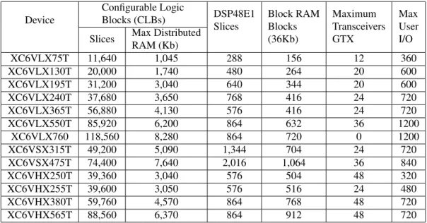
The Xilinx Virtex-6 SX475T FPGA with speed grade -1, which has been used in the dissertation, is part of the Virtex-6 SXT subfamily, which was designed to deliver the highest ratio of DSP and memory resources for high-performance applications.
The most important parameters of the Virtex-6 familiy are summarized in Table 2.1.
The chip contains74400slices,2016multiplier blocks (DSP48E1),38304Kb on-chip memory (BRAM), 2interface blocks for PCI express,4Ethernet MACs,840general purpose I/O blocks and36GTX transceivers.
To estimate the computational performance of the selected FPGA, we can assume a heavily pipelined architecture that is not memory bandwidth limited, e.g. dense matrix- matrix multiplication. In this type of applications, the performance is only limited by the number of operation units that can be implemented. To estimate the fixed point performance, the Xilinx LogiCORE IP Multiplier soft IP can be assumed as the basic operation unit. If it is configured to a fixed point 25x18 multiplier, it can be operated at 450MHz and occupies1DSP48E1 blocks. In this configuration,2016multipliers can be implemented, and each can start a combined multiply-and-add operation (MAD) for every clock cycle resulting in1814.4 giga operations per second. To estimate the floating-point performance, the Xilinx LogiCORE IP Floating-Point Operator can be used. In single precision case, it can operate at429MHz and occupies3DSP blocks.
In the selected FPGA, 672 multiplication units can be implemented and the remaining logic still allows 509 adder units, which can be connected to the multipliers resulting in436.7GFlops performance. In double precision case, the multiplication can operate at429MHz and occupies11DSP blocks. There are enough resources for 183 multipli- cation and adder units, however, the adder unit can operate at only361MHz resulting in132.1GFlops performance.
2.2 Graphical Processing Units
After the introduction of the unified shader architecture, the fast development of the GPU architecture has been continued. The next move toward general-purpose com- puting happened in late 2007, when AMD introduced the double-precision support in Radeon HD 3800 series and FireStream 9170. In 2008, the double-precision support
Table 2.1: Virtex-6 FPGA Feature Summary
Device
Configurable Logic
Blocks (CLBs) DSP48E1 Slices
Block RAM Blocks (36Kb)
Maximum Transceivers GTX
Max User I/O Slices Max Distributed
RAM (Kb)
XC6VLX75T 11,640 1,045 288 156 12 360
XC6VLX130T 20,000 1,740 480 264 20 600
XC6VLX195T 31,200 3,040 640 344 20 600
XC6VLX240T 37,680 3,650 768 416 24 720
XC6VLX365T 56,880 4,130 576 416 24 720
XC6VLX550T 85,920 6,200 864 632 36 1200
XC6VLX760 118,560 8,280 864 720 0 1200
XC6VSX315T 49,200 5,090 1,344 704 24 720
XC6VSX475T 74,400 7,640 2,016 1,064 36 840
XC6VHX250T 39,360 3,040 576 504 48 320
XC6VHX255T 39,600 3,050 576 516 24 480
XC6VHX380T 59,760 4,570 864 768 48 720
XC6VHX565T 88,560 6,370 864 912 48 720
also appeared at NVidia in the second generation of the unified shader architecture, called Tesla architecture. Traditionally, the GPU cards containing the GPU chip were connected to the host system via a PCI express slot and to the monitor via a video display interface, however, starting from these new architectures, both GPU manufac- turers started to offer special cards without video display for general-purpose high- performance computing.
For programming GPUs, both manufacturers introduced their own development platforms: CUDA SDK by NVidia and Stream SDK by AMD. In 2008, OpenCL, a general framework for writing programs which can be executed on various parallel architectures, was introduced. AMD decided to support OpenCL instead of its previous framework, while NVidia decided to support both OpenCL and CUDA. Although the OpenCL framework has the theoretical advantage that it can create universal program code, the performance of the universal code is sometimes far behind the native solution.
Usually, even in OpenCL, some hardware specific adjustments have to be done in the code to create a high-performance implementation, which leads to the following questions: Is it possible to describe wide range of architectures without a significant loss in the performance? Will OpenCL compilers be smart enough to compete with the native SDKs?
In the dissertation the NVidia K20 GPU has been selected for the demonstration of
viding more than one teraflops performance in double-precision and can be regarded as an illustrative example representing the modern GPU architecture. In the following section, the NVidia Kepler architecture, on which the K20 is based, is presented in more detail. As the DMRG program was implemented via CUDA, the CUDA SDK is also introduced.
2.2.1 NVidia Kepler architecture
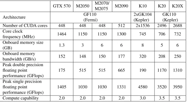
The Kepler architecture was released in 2012 and it can be regarded as the 4th ma- jor improvement of the GPU architecture since the introduction of the unified shader architecture. Compared to the previous generation (called Fermi), the manufacturer primarily focused on the minimization of the power consumption, and in the high- performance GK110 chip the double-precision performance was also increased. The main parameters of the NVIDIA Tesla products built upon the Kepler or the Fermi architectures are summarized in Table 2.2. The new architecture was reported 3 times more power efficient than the Fermi architecture [19] and introduced several new fea- tures, such as Dynamic Parallelism or NVidia GPUDirect. Dynamic Parallelism en- ables the programer to write smarter kernels which can dispatch new kernels with- out host intervention. NVidia GPUDirect is a new communication way, in which the GPU memory can be directly accessed via the PCI express interface eliminating CPU bandwidth and latency bottlenecks. The GPU can be directly connected to anetwork interface controller(NIC) to exchange data with other GPUs viaRemote Direct Mem- ory Access(RMDA). The GPU can also be connected to other 3rd party devices, e.g.
storage devices.
2.2.1.1 The general structure
A schematic block diagram of the Kepler GK100 chip is displayed in Figure 2.3. The chip is associated with CUDA Compute Capability 3.5, which is the revision number of the underlying architecture and determines the available CUDA features. The archi- tecture contains 15 Streaming Multiprocessors (SMX) and 6 64bit memory controllers.
Each SMX contains 192 single-precision CUDA cores, 64 double-precision units, 32 special function units, 65356 32bit registers, 64 KB shared memory, 48 KB read-only
Table 2.2: NVIDIA Tesla product line and the GTX 570 GPU, which was also tested in the dissertation.
GTX 570 M2050 M2070/
M2075 M2090 K10 K20 K20X
Architecture GF110
(Fermi)
2xGK104 (Kepler)
GK110 (Kepler) Number of CUDA cores 448 448 448 512 2x1536 2496 2688 Core clock
frequency (MHz) 1464 1150 1150 1300 745 706 732
Onboard memory size
(GB) 1.3 3 6 6 8 5 6
Onboard memory
bandwidth (GB/s) 152 148 150 177 320 208 250
Peak double precision floating point
performance (GFlops)
175 515 515 665 190 1170 1310
Peak single precision floating point
performance (GFlops)
1405 1030 1030 1331 4580 3520 3950
Compute capability 2.0 2.0 2.0 2.0 3.0 3.5 3.5
data cache, and 4 warp schedulers. SMX supports the IEEE 754-2008 standard for single- and double-precision floating-point operations (e.g. fused multiply-add) and can execute 192 single-precision or 64 double-precision operations per cycle. Special function units can be used for approximate transcendental functions such as trigono- metric functions.
2.2.1.2 CUDA programming
The CUDA SDK, which was debuted in 2006, is a general computing framework and a programing model that enables developers to program the CUDA capable devices of NVidia. Programs running on CUDA capable devices are calledkernels. Kernels are programmed in CUDA C, which is a standard C with some extensions. Kernels can be dispatched from various supported high-level programming languages such as C/C++
or Fortran, and there are also CUDA libraries, which collect kernels written for specific applications (e.g. CuBLAS for Basic Linear Algebra Subroutines).
When a kernel is dispatched, several threads are started to execute the same kernel code on different input. The mechanism is called Single Instruction Multiple Threads (SIMT), and one of the key differences from Single Instruction Multiple Data (SIMD)
Figure 2.3: A schematic block diagram of the Kepler GK110 chip. Image source: NVidia Ke- pler Whitepaper [19]. The chip contains 15 Streaming Multiprocessors (SMX). Cache mem- ories, single-precision CUDA cores, and double-precision units are indicated by blue, green, and orange, respectively.
is that threads can access input data via an arbitrary input pattern. Threads are or- ganized into a thread hierarchy, which is an important concept in CUDA program- ming. The programmer can determine the number and the topology (1D, 2D, or 3D) of threads to form athread blockand several thread blocks can be defined to form a grid.
The total number of threads shall match to the size of the problem that the treads have to solve. During execution the tread blocks are distributed among the available stream processors.
The second important concept in CUDA programming is the memory hierarchy.
At thread level, each thread can use private (local) registers allocated in the register file of SMX, which is the fastest memory. At thread block level, threads of a block can reach ashared memoryallocated in the shared memory of SMX. Finally, at grid level, all threads can access the on-board DDR memory, which is the largest but slowest memory on the GPU card.
When thread blocks are assigned to an SMX, the threads of the assigned blocks can be executed concurrently; even execution of threads of different blocks can be overlapped. The SMX handles the threads in groups of 32, called warps. The SMX distributes the warps between its four warp schedulers, and each sheduler schedules the execution of the assigned warps to hide various latencies. Each scheduler can issue two independent instructionsfor one of its warps per clock cycles, that is, an SMX can issue eight instructions per clock cycle if the required instruction level parallelism and functional units are available. As a warp contains 32 threads, one instruction cor- responds to 32 operations. To give an example, 6 single-precision instructions can be executed on the 192 CUDA cores and 2 double-precision instructions can be exe- cuted on the 64 double-precision computing units. As there is no branch prediction, all threads of a warp shall agree on their execution path for maximal performance.
2.2.1.3 NVidia K20
The NVIDIA Tesla K20 graphics processing unit (GPU), which is utilized in the disser- tation, is an extension board containing a single GK110 chip. The board is connected to the host system via an x16 PCI Express Generation 2 interface, which provides 8 GB/s communication bandwidth. The board contains 5 GB GDDR5 memory, which is
timated power consumption of the full board during operation is approximately 225 W.
Chapter 3
Solving Partial Differential Equations on FPGA
3.1 Computational Fluid Dynamics (CFD)
A wide range of industrial processes and scientific phenomena involve gas or fluid flows over complex obstacles, e.g. air flow around vehicles and buildings, the flow of water in the oceans or liquid in BioMEMS. In such applications, the temporal evolution of non-ideal, compressible fluids is often modeled by the system of Navier-Stokes equations. The model is based on the fundamental laws of mass-, momentum- and energy conservation, including the dissipative effects of viscosity, diffusion and heat conduction. By neglecting all non-ideal processes and assuming adiabatic variations, we obtain the Euler equations.
3.1.1 Euler equations
The Euler equations [20, 21], which describe the dynamics of dissipation-free, invis- cid, compressible fluids, are a coupled set of nonlinear hyperbolic partial differential equations. In conservative form they are expressed as
∂ρ
∂t +∇ ·(ρv) = 0 (3.1a)
∂(ρv)
∂t +∇ ·
ρvv+ ˆIp
= 0 (3.1b)
21
∂E
∂t +∇ ·((E+p)v) = 0 (3.1c) wheretdenotes time, ∇is the Nabla operator,ρis the density,u, v are thex- andy- component of the velocity vectorv, respectively,pis the thermal pressure of the fluid, Iˆis the identity matrix, andEis the total energy density defined by
E = p γ−1 +1
2ρv·v. (3.1d)
In equation (3.1d) the value of the ratio of specific heats is taken to beγ = 1.4.
The quantities ρ, ρv, E can be grouped into the conservative state vector U = [ρ, ρv, E]T, and it is also convenient to merge (3.1a), (3.1b) and (3.1c) into hyperbolic conservation law form in terms ofUand the flux tensor
F=
ρv ρvv+ ˆIp (E+p)v
(3.2)
as:
∂U
∂t +∇ ·F= 0. (3.3)
The equation expresses the conservation of quantityU: the change ofUequals to the divergence ofFwhich describes the transport mechanism ofU.
3.1.2 Finite volume method solution of Euler equations
Finite Volume Method (FVM) is a frequently used discretization strategy to numeri- cally solve the hyperbolic conservation laws expressed by the Euler equations [22]. To illustrate a possible application, a simulation of the airflow inside a scramjet engine is presented in Figure 3.1. During the discretization, a mesh is introduced for thecompu- tational domainwhere the PDE is studied. The idea behind the strategy is to integrate Equation 3.3 for each element (cell) of the mesh. Using the divergence theorem, the change of the quantity U inside each cell can be approximated via the fluxes going through the border of the cell:
Z
T
∂U
∂t + I
T
F·nT = 0. (3.4)
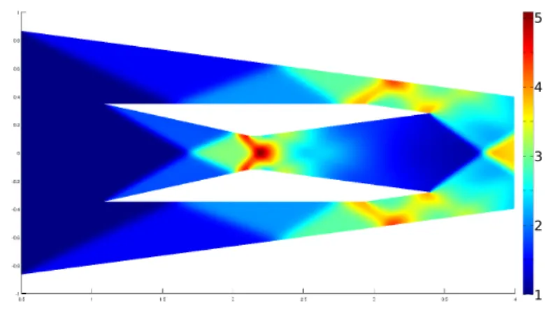
Figure 3.1: A simulation of the airflow inside a scramjet engine. Colors represent the value of the density (kg/m3) component of the state vector.
wherenTis the outward pointing unit normal field of the boundary of cellT. As numer- ical fluxes are locally conserved, flux computations can be reused in the neighboring cells.
The temporal derivative is discretized by the first-order forward Euler method:
∂U
∂t = Un+1−Un
∆t , (3.5)
whereUn is the known value of the state vector at time leveln, Un+1 is the unknown value of the state vector at time leveln+ 1, and∆tis the time step. In the current im- plementation, constant time steps are used, however, a variable time step modification of the framework is also possible.
In Chapter 4 the developed design methodology is presented via the solution of the Euler equations in case of structured and unstructured space discretization. In both cases the fluxes are computed similarly, however, in the unstructured case, extra rota- tions are needed which makes the numerical scheme more complex. In the following part both schemes are presented.
3.1.2.1 Structured mesh
Kocsardi et al. [23] showed that logically structured arrangement of data is a convenient choice for an efficient FPGA-based implementation. Hereby I am shortly reviewing the
numerical scheme because it is used as a test case to demonstrate the AU generation capabilities of the presented framework.
The computational domainΩis composed ofn×mlogically structured rectangles (cells). The area of a cell T is denoted by VT, while a face f is described by the vector nf which is normal to the face f and its size equals to the area of the face.
The flux tensor evaluated at a facef is denoted byFf. Using the cell centered FVM discretization, the governing equations (Equation 3.4) can be described as
∂UT
∂t =− 1 VT
X
f
Ff ·nf, (3.6)
where the summation is meant for all four faces of cellT.
In order to stabilize the solution procedure, artificial dissipation has to be intro- duced into the scheme. According to the standard procedure, this is achieved by re- placing the physical flux tensor by a numerical flux functionF˜ containing a dissipative stabilization term. In the dissertation the simple and robust Lax-Friedrichs numerical flux function is used, which is defined as
F˜ = FL+FR
2 −(|¯u|+ ¯c)UR−UL
2 (3.7)
where FL(UL) and FR(UR) is the flux at the left and right side of the interface, respectively, |¯u| is the average value of the velocity, and |¯c| is the speed of sound at the interface.
Fixing the coordinate system for each cell in an east-south direction, the dot product with the normal vector can be simplified to a multiplication by the area of the face. In case of eastward and southward fluxes the first and second columns of the flux tensor can be used, respectively:
F˜eastρ = ρLuL+ρRuR
2 −(|¯u|+ ¯c)ρR−ρL
2 (3.8a)
F˜eastρu = (ρLu2L+pL) + (ρRu2R+pR)
2 −(|¯u|+ ¯c)ρRuR−ρLuL
2 (3.8b)
F˜eastρv = ρLuLvL+ρRuRvR
2 −(|u|¯ + ¯c)ρRvR−ρLvL
2 (3.8c)
F˜eastE = (EL+pL)uL+ (ER+pR)uR
2 −(|¯u|+ ¯c)ER−EL
2 (3.8d)
F˜southρ = ρLvL+ρRvR
2 −(|¯u|+ ¯c)ρR−ρL
2 (3.9a)
F˜southρu = ρLuLvL+ρRuRvR
2 −(|¯u|+ ¯c)ρRuR−ρLuL
2 (3.9b)
F˜southρv = (ρLv2L+pL) + (ρRvR2 +pR)
2 −(|¯u|+ ¯c)ρRvR−ρLvL
2 (3.9c)
F˜southE = (EL+pL)vL+ (ER+pR)vR
2 −(|¯u|+ ¯c)ER−EL
2 (3.9d)
where L indicates the cell where the state vector is updated, while R indicates the neighboring cell (e.g. east or south). In case of northward and westward fluxes, the flux has already been computed at one of the neighboring cells and can be reused with a minus sign. Applying time discretization and using the numerical fluxes the state vectors can be updated according to the following formula:
Un+1T =UnT − ∆t VT
X
f
F˜f|nf|, (3.10)
3.1.2.2 Unstructured mesh
Structured data representation is not flexible for the spatial discretization of complex geometries. One of the main innovative contributions of our paper [1] was that an unstructured, cell-centered representation of physical quantities was implemented on FPGA. In the following paragraphs the mesh geometry, the governing equations, and the main features of the numerical algorithm are presented.
The computational domainΩis composed of non-overlapping triangles. Each face f of a triangleT is associated with a normal vectornf which points outward T and is scaled by the length of the face. The volume of a triangle T is indicated by VT. Following the finite volume methodology, the state vectors are stored at the mass center of the triangles.
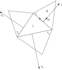
During flux computation the coordinate system is attached to the given facef such a way that axisxis normal tof(see Fig. 3.2). The benefit of this representation is that theFf·nf dot product equals to the first column ofFmultiplied by the area of the face.
The drawbacks of the representation are that the velocity vectors have to be rotated to this coordinate system before the flux computation and fluxes have to be rotated back to the global coordinate system before final summation.
Figure 3.2: Interface with the normal vector and the cells required in the computation
Similarly to the structured case, the Lax-Friedrichs numerical flux function (Equa- tion 3.7) is used to stabilize the solution, however, in this case, the normal component of the numerical flux function has to be calculated for each interface:
F˜fρ = ρLuL+ρRuR
2 −(|¯u|+ ¯c)ρR−ρL
2 (3.11a)
F˜fρu = (ρLu2L+pL) + (ρRu2R+pR)
2 −(|¯u|+ ¯c)ρRuR−ρLuL
2 (3.11b)
F˜fρv = ρLuLvL+ρRuRvR
2 −(|¯u|+ ¯c)ρRvR−ρLvL
2 (3.11c)
F˜fE = (EL+pL)uL+ (ER+pR)uR
2 −(|¯u|+ ¯c)ER−EL
2 (3.11d)
where L indicates the cell where the state vector is updated and R indicates the neigh- boring cell.
Applying time discretization and using the numerical fluxes, the state vectors can be updated according to the following formula:
Un+1T =UnT − ∆t VT
X
f
RˆnfF˜f|nf|, (3.12)
whereRˆnf is the rotation tensor describing the transformation from the face-attached coordinate system to the global one. Unfortunately, in the unstructured case, it is not
memory requirement of the implementation.
The AU is generated from Equations 3.11a to 3.11d and is designed to compute the normal component of the numerical flux function for a new interface in each clock cycle. Beside the AU an additional simple arithmetic unit is required to update conser- vative state variables (ρ, ρu, ρv, E) using the flux vectors. As a cell has three interfaces, three clock cycles are required for a complete cell update.
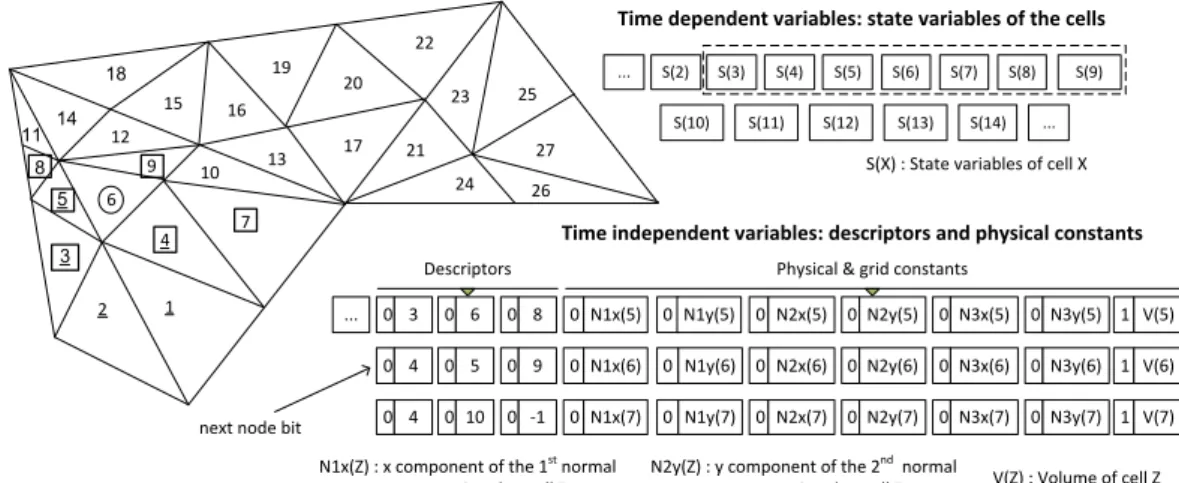
3.2 Data structures and memory access patterns
The data structures used in the presented architecture were designed to efficiently use the available memory bandwidth during transmission of the unstructured mesh data to the FPGA. In numerical simulations data is discretized over space and can be rep- resented at the vertices of the mesh (vertex centered) or the spatial domain can be partitioned into discrete cells (e.g. triangles) and the data is represented at the center of the cells (cell centered). From the aspect of accelerator design both vertex and cell centered discretization can be handled with a very similar memory data structure and accelerator architecture. In both cases the data can be divided into a time dependent (state variables) and a time independent part which contains mesh related descriptors (e.g. connectivity descriptor) and physical constants.
In the solution of the CFD problem which is presented in the dissertation, the cell centered approach is used, therefore the proposed data structures are explained for this case. In Figure 3.3 an example of an unstructured mesh is shown, in which the cells are ordered, and the computation of the new state values is carried out in an increas- ing order. Already processed cells are indicated by underlined numbers, the currently processed cell is encircled and squared cells are currently stored in the on-chip mem- ory. On the right side of the figure, fragments of the appropriate data structures are illustrated.
Time dependent variables are composed of the state variables associated to the cells. When a cell is processed, the state variables are updated based on the state vari- ables of the given cell and its neighborhood (discretization stencil). State variables are transmitted to FPGA in processing order and can be stored in a fixed-size shift register (on-chip memory). When a cell is processed, all the state variables of the cells from the
11 8
20 14
5
15
3
16
18 19
22
23 25
27 24 26 17 21
10 13
7 4
1 12
9 6
2
S(3)
...
...
...
next node bit
Time dependent variables: state variables of the cells
Time independent variables: descriptors and physical constants S(X) : State variables of cell X
S(4) S(5) S(6) S(7) S(8) S(9)
S(10) S(11) S(12) S(13) S(14)
S(2)
0 8 0 N1x(5) 0 N1y(5) 0 N2x(5) 0 N2y(5) 0 N3x(5) 0 N3y(5) 1 V(5) 0 6
0 3
0 9 0 N1x(6) 0 N1y(6) 0 N2x(6) 0 N2y(6) 0 N3x(6) 0 N3y(6) 1 V(6) 0 5
0 4
0 -1 0 N1x(7) 0 N1y(7) 0 N2x(7) 0 N2y(7) 0 N3x(7) 0 N3y(7) 1 V(7) 0 10
0 4 ...
V(Z) : Volume of cell Z N1x(Z) : x component of the 1st normal
vector associated to cell Z
N2y(Z) : y component of the 2nd normal vector associated to cell Z
Physical & grid constants Descriptors
Figure 3.3: On the left, an unstructured mesh is shown to illustrate which cells are stored in the on-chip memory. Indices of the cells indicate the order of computation. Already processed cells are indicated by underlined numbers, the currently processed cell is encircled and squared cells are currently stored in the on-chip memory. On the right, fragments of the appropriate data structures are presented.
neighborhood stencil must be loaded into the on-chip memory, however, cells which have no unprocessed neighbors can be flushed out. In the presented example, when cell 6 is processed, all the necessary state variables are in the fast on-chip memory of the FPGA. To process the next cell (7), a new cell (10) should be loaded, and cell 3 can be discarded from the on-chip memory. It is possible that multiple new cells are required for the update of a cell, indicating that the on-chip memory is undersized. The size of the required on-chip memory depends on the structure of the grid and the num- bering of the cells, consequently, a great attention should be paid for the ordering of the mesh points in a practical implementation. In the presented cell centered example the neighborhood stencil is relatively simple, however, more complicated patterns can be handled in the same way.
Time independent variables are composed of mesh related descriptors and other physical constants which are only used for the computation of the currently processed cell. They mainly differ from the time dependent variables because they are stored only for the currently processed cell and they are not written back to the off-chip memory.
Consequently, time dependent and time independent data must be stored separately in
to the off-chip memory in bursts.
Mesh related descriptors describe the local neighborhood of the cell (vertex) which is currently processed. In unstructured grids, the topology of the cells (vertices) can be described by a sparse adjacency matrix, which is usually stored in a Compressed Row Storage (CRS) format [24]. As the matrix is sparse and the vertices are read in a serial sequence (row-wise), the nonzero elements can be indicated by column indices and anext node bit, which indicates the start of a new row (see Figure 3.3). In the 2D cell centered case, the descriptor of a cell is a list, which contains the indices of the neighboring cells, however, in others cases (e.g. vertex centered) additional element descriptor may be required. Boundary conditions can be encoded by negative indices in the connectivity descriptor as illustrated in case of cell 7. If the size of the descriptor list is constant, the next node bit can be neglected.
Time independent data also contain physical constants which are needed for the computation of the new state values. These constants can be appended after the de- scriptors as shown in Figure 3.3. In case of the demonstrated CFD problem these constants are the normal vectors indicating the edges of the cells (triangle) and the volume of the cells.
3.3 Structure of the proposed processor
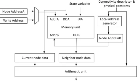
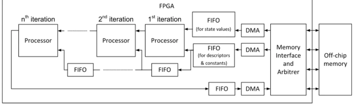
The processor were designed to efficiently operate on the input stream of the data of the ordered mesh points. The two main parts of the processor are the Memory unit and the Arithmetic unit (AU) as shown in Figure 3.4. The job of the Memory unit is to prepare the input stream and generate the necessary inputs to the AU, which should continuously operate and get new inputs in each clock cycle. The Memory unit could be reused with little adjustments if an other PDE needed to be solved, however, the AU would have to be completely reimplemented according to the new state equa- tions. Consequently, the presented automatic generation and optimization of the AU can drastically decrease the implementation costs of a new problem.
The Memory unit is built from dual ported BRAM memories and stores the state variables of the relevant mesh points. The minimal size of the on-chip memory is determined by the bandwidth of the adjacency matrix of the mesh. The bandwidth
![Figure 2.3: A schematic block diagram of the Kepler GK110 chip. Image source: NVidia Ke- Ke-pler Whitepaper [19]](https://thumb-eu.123doks.com/thumbv2/9dokorg/1308696.105279/35.892.175.765.409.770/figure-schematic-diagram-kepler-image-source-nvidia-whitepaper.webp)