Compound semiconductor layers for optoelectronic and photovoltaic purposes
PhD Thesis
Zsófia Baji
Supervisor:
Dr György Molnár
Budapest University of Technology and Economics and
Research Centre for Natural Sciences, Institute for Technical Physics and Materials science
2013
Contents
I. Introduction ... 3
1. Motivation... 3
2. Overview of the research field ... 5
2.1 Atomic Layer Deposition ... 5
2.2 Properties and preparation of ZnO layers ... 16
2.3 CIGS solar cells ... 23
3. Experimental methods ... 31
3.1 The atomic layer deposition system ... 31
3.2 Thermal evaporation and sputtering ... 32
3.3 Hall measurement ... 32
3.4 Spectroscopic ellipsometry ... 33
3.5 Microscopy ... 33
3.6 SNMS and XPS ... 34
3.7 XRD ... 35
3.8 UV-VIS transmittance spectroscopy ... 35
II. Results and discussion ... 36
4. Atomic layer deposition of Al doped ZnO layers ... 36
4.1 The structure and morphology of Al doped ZnO layers ... 38
4.1.2 The resistivity of the ALD deposited AZO layers ... 45
5. Nucleation and growth of atomic layer deposited ZnO layers ... 52
6. The growth of epitaxial ZnO layers ... 59
7. Deposition of CIGS layers with post selenization of the metallic components ... 66
7.1 The morphology of the evaporated metals ... 67
7.2 Post annealing of stacked metallic layers ... 70
7.3 Selenization of metallic components with Se vapour ... 73
7.4 Post selenization of flash evaporated metallic layers ... 77
Summary ... 82
Theses ... 84
List of abbreviations ... 87
Acknowledgement ... 88
References ... 89
I. Introduction 1. Motivation
Solar cells, as most members of renewable energy production, have recently been gaining a growing interest. Due to reports on global warming and energy needs the importance of developing new technologies in a cost-competitive way is the main motivation of thin film solar cells research.
As the visible light spectrum is between 1.6-3.4 eV, the active layer of a solar cell needs to have a band-gap not exceeding these values. A number of materials fulfil this requirement, and result in solar cells with various efficiencies and costs. The great advantage of thin film solar cells is that they have a low material requirement. The active layer of these devices has a thickness in the range of a few microns between two glass panes.
My theses focuses on thin films of two materials, both crucial for a number of photovoltaic applications: CIGS (Cu(InGa)Se2), which is the absorber material of one of the most promising thin film solar cell family, and ZnO, which is the most commonly used transparent electrode material. As a wide band-gap semiconductor ZnO is also important for a number of optoelectronic applications as well.
CIGS materials are one of the most popular members of the thin film solar family as they combine cost efficiency with stability and a reasonably good efficiency. (20% for CIGS in laboratory scale)[1.1]. They can be prepared with a number of methods, but the processes that result in the best efficiency cells are extremely complex. Therefore there is a perspective of improving the fabrication of such solar cells significantly by the application of more economical and simpler deposition methods. The post selenization of copper, indium and gallium precursors is one of the most promising new directions for chalcopyrite fabrication. This technique is extremely simple and no expensive apparatus is needed, as the process is defined by the stoichiometry, and the parameters do not require precise tuning.
ZnO is a material with a direct band-gap of 3.37 eV, an exciton binding energy of 60 meV, and a very high radiation and thermal stability. It is piezoelectric, and can even be ferromagnetic if doped with transition metals. Unfortunately, up to now the lack of good quality single crystalline ZnO has hindered the advances concerning this material, but recently epitaxial growth on GaN has renewed interest in it. On the other hand transparent conductive oxides are crucial for a number of optoelectronic and electronic device applications as well, due to their very high exciton binding energy (60meV) [1.2]. A few examples are as TFTs, LEDs, field emitters, and flexible electronic devices. This application would require the growth of high quality epitaxial layers, preferably with a tuneable band gap and resistivity.
Another excellent application for ZnO would be as the buffer layer in CIGS solar cells.
Usually CdS is used as this thin film between the active layer and the window electrode, but it is highly toxic and environmentally hazardous. It is also very impractical as its wet deposition interrupts the vacuum process [1.3]. However, sputtered ZnO does not grow with the required conformity on the CIGS film, therefore the use of a buffer layer is indispensable. Atomic layer deposited (ALD) ZnO would be
a vacuum-compatible alternative, which even meets the requirements on conformality, uniformity and reproducibility.
In the case of organic and hybrid solar cells it is crucial that the transparent conductive electrodes are always within a diffusion length from the location where the charges were generated. This requires high quality transparent conductive oxide materials grown in a number of high aspect ratio and surface/volume ratio structures on a nanometre scale. ALD ZnO is a perfect candidate to fulfil this immensely high requirement.
The aim of the present work is therefore to examine the basic qualities and physical properties of thin films of two chosen materials: ZnO and Cu(In,Ga)Se2.
On the one hand to examine the basic physics of ALD deposited ZnO layers. The systematic investigation of Al doping and its effects on the conductivity is aimed, and the elaboration of novel structures from ALD ZnO for solar cell and opto-electronic purposes is targeted.
On the other hand new, cheaper and simpler methods were tried to deposit the CIGS active material. One of the possibilities is the post-selenization method, that is, to anneal the CuInGa metals in Se atmosphere. This is an easily available method that enabled us to examine the processes and physical phenomena that take place during the selenization process of metallic precursors, and the required parameters of the absorber material.
2. Overview of the research field
2.1 Atomic Layer Deposition
Atomic layer deposition (ALD) is a self-limiting layer by layer growth method. It was invented by Tuomo Suntola et.al. [2.1.1.], and was first used for the deposition of epitaxial layers of compound semiconductors. Hence the original name of the method: atomic layer epitaxy. The low growth rate limited the applications at first, but with the further size reduction of semiconductor device dimensions the method gained a renewed interest. Nowadays it is considered to be one of the most promising thin film and nano-structure fabrication methods. Further improvements to the technique have made it possible to grow a huge number of compound materials and even elements can be grown. Also, due to a low growth rate and the governing chemisorption process, an epitaxial growth of a number of materials can relatively easily be achieved with the ALD method with a proper tuning of the growth parameters [2.1.2].
The operation principle of the technique is very similar to that of CVD growth: it is based on the introduction of precursor gases into the vacuum chamber, and their subsequent deposition on a heated substrate surface. The difference is that here the precursors are consecutively introduced into the reactor, and between the precursor pulses the reactor is purged by an inert gas. Therefore they can only react with the substrate surface and never with one another in gas phase, which prevents the formation of particles in the gas phase that could be adsorbed on the surface and build a granular film. The chemisorption on the heated substrate surface ensures a uniform and conformal coverage independent of the surface morphology. This means that any given aspect ratio substrate may be evenly coated by this method, in an ideal case even after just one mono-layer of deposition. As the surface reactions are self-limiting, one deposition cycle always forms only one mono-layer of the grown compound on the saturated surface. With the sequential repetition of the deposition cycles conformal and uniform films may form at an atomic layer control.
The self-terminating characteristic of the method also means that the precursor fluxes need not be uniform, only a saturated chemisorption has to be achieved. At the same time the composition of the layer can be tailored under a nanometre scale [2.1.3].
The advantages of the ALD method
The versatility of the ALD method is especially important in micro-technology, where, due to the miniaturization, extremely thin films are required with their composition and uniformity controlled at an atomic level. Also in micro-technology complicated structures with extremely high aspect ratios need to be covered with continuous layers.
As a summary, the main advantages of the method are:
conformal and uniform coverage
possibility to coat high aspect ratio structures
precise thickness and composition control
easy and precise doping
pinhole free layers
easy scale-up
low temperature deposition
possibility of growing epitaxial layers
The ALD growth
Fig 2.1.1. explains the ALD process through the ALD sequence for ZnO deposition.
The deposition steps are the following:
1. First, diethyl-zinc, the metalorganic precursor for Zn, is introduced into the reactor
2. It chemisorbs on the substrate surface, one of its C2H5 ligands reacts with the hydrogen from the surface OH groups, and thus the Zn connects to the oxygen.
3. Afterwards, an inert gas (typically nitrogen) purges the unreacted precursor residue and the ethylene out of the chamber.
4. Next, the oxidant (usually water vapour) is introduced. It reacts with the Zn on the substrate surface, giving a H ion to the other C2H5 ligand, resulting in a C2H6
molecule.
5. Then a final purging clears out the reactor and the result of the growth cycle is one mono-layer of ZnO [2.1.4].
Fig. 2.1.1. The Atomic layer deposition cycles of ZnO
The tuning of the deposition parameters means the setting of the deposition temperature, the gas flow rates and purging times so that the growth rate is stable and constant. The purging times are especially important, because if they are not set long enough, the precursors meet in gas phase as well, and a CVD-like growth occurs.
The growth rate depends strongly on the deposition temperature. It affects both the number of adsorption sites on the substrate, and the quality of the chemical reactions that take place on the surface.
The range of the ideal growth temperatures is the so-called ALD window, which is shown in fig. 2.1.2. As the idea of the method means that only chemisorption is
possible, it is necessary that the adsorbates only form strong bonds with the surface.
At the temperature of the deposition any bond between the adsorbate molecules has to be weak. At the temperature range below the ALD window the growth rate may increase with the temperature, if the precursors need an activation energy to form bonds with the substrate surface and each other. In some cases though, the growth per cycle decreases with the increasing temperature in the low temperature regime.
This is due to a low temperature multi-layer growth by physisorption with the precursors simply condensing on each other. At too high temperatures once again the growth rate may increase or decrease with the temperature. In most cases it decreases as the adsorbed molecules now have enough energy to desorb again after adsorption. On the other hand an increasing growth may be experienced if the temperature is so high that the adsorbate molecules form bonds with each other, and particles form, which results in a higher than one molecular layer per cycle growth rate. In this case the deposition is not atomic layer controlled; this region is also called the CVD region [2.1.3].
Fig 2.1.2. The ALD window of the ideal growth
Even within the ALD window, that is, within the temperature range where the layer growth is stable and self-limiting, the growth per cycle depends on the temperature.
Increasing the temperature may decrease the growth rate, typically through decreasing the number of adsorption sites. The growth rate may also increase with the temperature if the higher temperature provides extra energy, which is then sufficient to overcome some barrier, and another type of reaction may start. The growth rate-temperature connection may be constant, if the available sites are not the limiting circumstances, but the steric hindrance is. The growth- temperature relation may also grow to a certain point, and then decrease. This is usually the case, if the typical surface reactions need a certain activation energy that can be provided by the heat, but by further increasing the temperature the available reactive sites start to decrease.
The morphology and the crystallinity of the layers are determined by the surface mobility of the material, through which also by the temperature, and the crystalline structure of the substrate. The choice of precursor materials only has an effect on these qualities in rare cases (e.g. TiO2 films show superior qualities if deposited from titanium alkoxides). The crystallinity of the layers may be tuned with the
temperature ranging from amorphous to different crystalline structures (as in the case of -once again- TiO2 which grows amorphous at low temperatures, then in anatase structure, and at temperatures above 300° as rutil). The crystalline orientation may also be influenced by the growth temperature. Polycrystalline film growth always results in rough films with a roughness in the range of nanometres and increasing with the film thickness [2.1.5].
Coating high aspect ratio structures
Atomic layer deposition is an outstandingly versatile method to coat arbitrary ultrahigh aspect ratio structures [2.1.6, 2.1.7]. Due to the chemisorption a full coverage can be expected over the whole surface, even at the bottom of high aspect ratio holes if the precursor exposures are high enough for all the reactant gases to diffuse into and out of the holes. George et al. [2.1.8] developed a model to describe the coverage of high aspect ratio structures by ALD. Using a Monte Carlo simulation they found that depending on the sticking coefficient and the aspect ratio, the coating of the pores could be diffusion or reaction controlled, which two cases lead to different coverage profiles. The process is reaction controlled if S<<H, where S is the sticking coefficient and H=16(d/L)2, with d/L being the aspect ratio. In this case the holes are filled randomly and the reactants fill the space evenly before reacting.
In the diffusion limited regime when S>>H, the pores are filled up inwards from the opening of the pore with an abrupt boundary between the coated and uncoated parts, and the process is independent of the value of S. In this case the coverage has a t1/2 time dependence. For the diffusion controlled case the minimum exposure times for the conformal deposition on high-aspect-ratio pores could be determined generally, and be applied to various ALD surface chemistries. The reactive sticking coefficients (the probability that an incoming molecule sticks to the surface) are S=10-3 for Al2O3, and 7*10-3 for ZnO. The expected exposure times for the case of DEZ are shown in fig. 2.1.3.a.
Fig. 2.1.3. b and c show my experiments on some high aspect ratio structures:
Fig. 2.1.3 a: the required exposure times vs aspect ratio, from [2.2.10]. b: DRIE
etched holes coated with 50 nm thick ALD ZnO, c: porous silicon with a typical pore size around 50nm, coated with 5 nm ALD ZnO
The growth rate
A common misunderstanding about the atomic layer deposition is that the growth actually takes place mono-layer by mono-layer, which would indicate a growth rate of one lattice spacing in each cycle. In the case of chemisorption controlled processes a mono-layer is generally defined as the amount of adsorbates that occupies all the available sites on the substrate surface. This means that the mono- layer is considered complete if further growth is impossible, even if a full molecular layer of a crystal has not yet been grown. In reality the growth rate is almost never one full molecular layer per cycle. The ALD window and the tuning of the deposition parameters means that the reactant is in saturation, therefore the only hindering process is that of the chemisorption.
The chemisorption process itself must always be irreversible for ALD purposes, that is, once an adsorbate connects to the surface, it must not desorp again. The chemisorption may commence through three different mechanisms: Ligand exchange, where the reactant arrives at the surface, releases a ligand, and then further ligands get consumed via reactions with surface groups; dissociation, where a reactant molecule is split upon reaching the surface thus engaging two or more surface groups; association, when the reactive molecule forms a coordinative bond with a surface site without releasing ligands.
Two processes always hinder the chemisorption and define the saturation of the surface: the number of connecting sites on the surface, and the steric hindrance of the precursor molecules. The number of available sites on the surface might not be enough to achieve a full mono-layer of the grown crystal, or the adsorbate molecules might be so large, that they engage more than one connection site. A third hindering process that occurs at times is that bulky ligands of a chemisorbed precursor molecule get adsorbed on the surface, thus engaging bonding sites, and further hindering the growth by their steric hindrance. Nevertheless, the chemisorption coverage is considered complete, after a self-termination has been achieved [2.1.7].
The most detailed model describing the growth rates experienced during ALD depositon has been developed by Ylilammi [2.1.9], and considers both the adsorbate sizes, and a substrate surface structure. During the adsorption of the precursors their size and the available bonding sites define the maximum density of the adsorbate molecules. The latter depends on the crystalline structure of the surface.
This can be very different in amorphous or crystalline substrates, but even the surface of crystalline samples experiences some reconstruction. The dislocations or impurities also influence the nucleation, while a roughness increases the area of the surface [2.1.10]. The precursors used in ALD processes are often large. We can assume that the adsorbates occupy the surface in the densest possible distribution.
The packing density is the ratio of the adsorbed atoms to the adsorption sites occupied. This is the process through which the steric hindrance affects the growth rate. On the other hand the surface coverage may not be complete if the surface chemistry also hinders the process. Calculating the packing density is
straightforward according to [2.1.9]. As the molecules may rotate around the bonding sites, we may approximate their geometry with circles. The packing density depends on the ratio of the distance between the adsorption sites, and the size of the adsorbates. However, the first step of the adsorption, before the chemisorption, is when the molecules physisorb on the surface, therefore they cannot get too close to each other, as the repulsion between the adsorbates is stronger than the physisorption.
Due to the above-mentioned effects the growth per cycle in atomic layer deposition is always considerably less than a mono-layer. In fact a growth of 0.5 atomic spacing per deposition cycles is regarded as very high [2.1.10].
The nucleation is also a crucially important factor of the initial phase of the growth as the ALD process can only start if there are adequate chemical species to which the precursors may connect. If the surface is inert, the reaction may only start at defect sites and an island-like growth takes place at the initial stages of the film growth.
Having the islands grown together a stable growth rate sets in, and a uniform layer- by-layer growth starts. Note, that in the initial stages of growth, in the first few cycles, the layers are not continuous. This phenomenon occurs when the reactants grow rather on the ALD-grown material, and not so much on the substrate. It has been reported for instance in the case of Al2O3 growth on Si and carbon surfaces, e.g.
graphene [2.1.10]. Ref [2.1.11] also found agglomerates of ALD grown ZnS after the first few (~10) growth cycles, which then grew in size and then formed a continuous film with a very rough surface. A random deposition is also possible, where the landing of the adsorbate molecules is just as likely on the substrate as on the islands of the grown material.
During the first few cycles of growth the adsorption of the precursors is completely different from the later ones, as the reaction with the substrate surface might be different from the reaction with the material itself. Between these two there is a transient regime, where both the substrate surface and the ALD grown material surfaces are present. A substrate enhanced growth is possible if the substrate offers more reactive sites than the material surface, while in the case of substrate inhibited growth an island-like growth is also possible. It some cases the growth does not depend on this effect, and the growth rate is linear even in the initial phases of the growth.
The agglomeration of the adsorbed molecules can also occur if the system tries to minimize the interface energy between the two materials. In this case, after a mono- layer has been grown, the adsorbates can migrate and form islands. In fact, according to Ritala and Leskela this is a more likely explanation of the island-like growth in atomic layer deposition [2.1.5].
Another possible explanation is that during film growth certain intermediate species have a higher mobility on the surface, and they are responsible for the migration and the agglomeration.
Precursors in ALD
Precursor chemistry is a key question of ALD. The research is always active for new precursors, for example there is still no effective ALD process known for SiO2
deposition. The deposition of elements is always complicated as well, as it is especially challenging to find precursors reactive enough to reduce to elements with chemisorption to a surface simply by thermal assistance.
The reactants used in ALD should be volatile at a reasonable temperature achievable with the ALD instrumentation, should not decompose at the reaction temperature, and they should perform chemisorption and a reaction on a heated surface. This means that an especially strong reaction between them and the surface must be possible. On the other hand, the surface reactions must also be complete, even at low temperatures, and no residues should remain on the surface. Also, the by-products of the surface reaction must be un-reactive so that they can easily be swept out of the reactor. In rare cases an etching may occur between the pulses, especially in the case of multi-layer structures where the precursor of one component may etch back the deposited layer of the other. Another negative effect is the dissolution of the precursors into the substrate of the ALD deposited material. These phenomena are detrimental to the film growth and must be avoided.
The precursors can be gases, liquids or solids. As the ALD process does not require a homogeneous or constant flux, the only necessary requirement is that they should have a large enough vapour pressure at the required temperature. The source chemicals used in ALD may be used at room temperature, if their vapour pressure is sufficient to provide the required flux. These are kept in vessels, from which the vapour is led into the reactor directly and pulsed with fast operating valves. The lower vapour pressure materials need to be kept in boosters and heated to the required temperature [2.1.12, 2.1.13].
Applications of the ALD method
The ALD method is the most popular for growing composites, especially oxide and nitride films, but elements have also been grown. Nitride and oxide films grown by ALD are becoming more and more popular for microelectronic applications, such as diffusion barriers, and the new generation of gate oxides also offers an ideal application for ALD oxides. The very thin –nano-scale- oxides with high dielectric constants, an extreme smoothness and an engineered band-gap deposited by this method can be reliable gate layers. For this purpose avoiding the oxidation of the silicon surface during deposition is an important issue that can easily be solved in an ALD reactor by avoiding the use of highly oxidizing precursors. Multi-layer structures might also be used as high-k dielectrics [2.1.12].
Nitride films can be used as diffusion barriers in IC fabrication. Most common are perhaps TiN and TaN. The majority of the nitride layers are deposited from metal chlorides and ammonia, in which case the extremely low growth rate is an issue.
Elemental films, e.g. tungsten and copper can also be reliably grown with the ALD method. In this case reducing elements must be used as the other precursor. The material of choice for this role is generally hydrogen. For example Cu has been grown by a reaction of CuCl and H2. As H2 gas is sometimes not reactive enough at the substrate temperatures applied in ALD, atomic hydrogen must be produced by plasma or by thermal cracking. Plasma assisted ALD is highly reactive, and the deposition of numerous metals has been made possible by this approach. Even
metallic titanium and tantalum has been grown with this method at deposition temperatures of 25-400°C. The other possibility to enhance the growth of materials with a lower reactivity is by photo assistance, in which case the surface is enlightened with a UV source, and this gives the extra energy required for the chemisorption [2.1.12].
One great advantage of the ALD method is the deposition of high quality films at low growth temperatures. Due to the chemisorption the impurity concentration is expected to be quite low even at temperatures lower than 100°C. The heating of the substrate is important for all the surface reactions to take place, and the only disadvantage of the low temperatures is a slightly higher impurity level, but this is still low compared to CVD. Deposition of TiO2, SiO2 and Al2O3 films below 50°C has been reported in Refs. 2.1.14. and 2.1.15. The low temperature deposition is also advantageous as it makes the layer deposition on polymers and organic materials possible which could be a breakthrough for flexible electronics. The nucleation process on polymers is somewhat different from the conventional though, as there are no hydroxyl species on some polymer surfaces, therefore they do not have nucleation sites. The precursors in this case penetrate within the holes in the polymer and the nucleation then occurs on these absorbed molecules.
Another important characteristic of the ALD method is the ability to form nano- laminates easily. While depositing a composite material (e.g. an oxide) some precursor pulses have to be replaced by the dopant material. If the original was an ABAB pulse sequence, then the multi-layer can be fabricated following an (AB)x(CD)y sequence. The ratio of the x and y thickness of the two layers defines the composition of the multi-layer. If x and y are both large, we get an even multi-layer. If they are both small, the result will be a homogeneous alloy. However, if one is much larger than the other the film will be a slightly doped layer. On the other hand the deposition of compositionally modulated thin films can also be easily achieved with the ALD method. For example it is an ideal tool for the deposition of multi-layers for optics, where thin films with precisely controlled thickness and composition are required. Among the ALD grown materials dielectrics with a refractive index varying between 1.43 and 2.6 can be deposited, and even the growing films with graded refractive indices is fairly straightforward. Optical and X-ray mirrors have been made by ALD: In the soft X-ray wavelength range the layers have to be only a few nanometres thick, which is typically the challenge designed for the ALD method [2.1.16].
Due to the self-assembly characteristics of the process, ALD is an ideal tool for fabricating nano-structures. In this case the traditional approaches for lateral patterning need to be revised, but the ALD based nano-fabrication can easily be carried out with the use of nano-templates [2.1.17].
Due to the uniformity and the precise thickness control nano-coating is an excellent application for ALD [2.1.18]. Protective coating of nano-sized objects can be easily, reliably and reproducibly solved with the method. Min et. al. coated ZnO nano-rods with Al2O3 to protect them from contamination and corrosion. The nano-rods were 10-30µm long and 50-200 nm in diameter and they were covered with 45 nm Al2O3
uniformly [2.1.19].
The coating of nano-particles or nano-sized balls can be achieved with ALD, after which the particles themselves may be removed by an etching step, thus even hollow nano-sized balls can be made [2.1.20]. This method has an especially interesting application in the fabrication of three dimensional photonic crystals. These structures have a periodically varying dielectric constant, which results in the photons behaving somewhat like electrons in a crystal: a band structure is formed, in cases even with band-gaps, where photons cannot exist. 3D photonic crystals can be made by the self assembly of nano-spheres in an fcc order, and another material with a markedly different dielectric constant filling in the voids. The other approach is to make inverse photonic crystals, where the voids are filled with a high dielectric constant, and then remove the template nano-balls. Povey et.al. [2.1.21] fabricated photonic crystals with Al2O3 and VO2 void filling between silica spheres. Covering nano-particles is even simpler in fluidised bed reactors.
ALD reactors
ALD reactors of a number of designs exist, but they all consist of a reaction chamber with a substrate holder in it, and precursor gas inlets. The pressure within the reactor may range between ultrahigh vacuum to atmospheric pressure depending on the reactor type and design.
In the case of an ultrahigh-vacuum reactor with molecular flow the reactants can be introduced into the chamber, and then removed with a pump that evacuates the reactor. This makes an economical utilization of the precursors possible, but the deposition is relatively slow. The other construction carries the precursors with a neutral gas, and between the pulses the reactor is also purged with this inert gas.
These are the flow type reactors, which are usually preferred in industrial use as the deposition is incomparably faster with them. They usually operate under viscous flow conditions. In both reactor types it is crucially important for the walls of the reactor to be uniformly heated, as the precursors may adsorb on cold spots, which makes the purging or the evacuation a great deal harder. The carrier gas used in the reactors is an inert gas, usually nitrogen that has to be at least of 5.0 (99.999%) purity, as this is the main impurity source in the deposition.
Most reactors, especially for research purposes, are open tubular chambers, in which any type of substrates may be placed and arranged arbitrarily. The batch reactors on the other hand are usually designed in travelling wave arrangement. In this design the substrates are placed parallel with each other, with just a narrow space between them. The pulsing is then synchronised with the evacuation of the reactor so that the precursor pulse travels over the substrates like a wave front, and before it is pumped out of the reactor, the next pulse follows behind it with a purging wave between them. In this design the precursor molecules collide with the surfaces multiple times, and the substrates become saturated very quickly. This allows a very fast and cost efficient use. There is also another reactor design: that of the flow type reactors with moving substrates, where the movement of the substrates is synchronised with the precursor pulses.
The deposition of the precursors on the surface is usually helped with a heating of the substrate. This method is called thermal ALD. In cold wall reactors only the
substrate is heated, in hot wall reactors the whole chamber is heated to the deposition temperature. In the cases when the thermal energy is not enough to ensure the reaction of the precursors on the surface, the reaction may be assisted by a plasma source.
The scale up of the ALD process is very easy as only the saturation of the precursor gases need to be ensured, the laminar flow needs not be considered in the design.
Therefore batch reactors are already available in the market [2.1.3, 2.1.5].
2.2 Properties and preparation of ZnO layers
Wide band-gap semiconductors (e.g. GaN) are very suitable for the purposes of high power, high temperature electronic devices and short wavelength opto-electronics.
In fact, they may even be more suitable for these purposes than GaAs due to their superior qualities: they tend to have larger electron mobility, and higher breakdown field strength. ZnO is a material with a direct band-gap of 3.37 eV, which means it is still transparent in UV light. On the other hand its exciton binding energy is 60 meV, which increases the luminescence efficiency. (In comparison, the exciton binding energy of GaN is 25 meV.) The room temperature Hall mobility can be as high as 200 cm2/Vs in mono-crystalline samples whereas the carrier concentration in the intrinsic case is typically in the order of magnitude of 1015-1018 /cm3. ZnO also has a very high radiation and thermal stability. It is piezoelectric, and can even be ferromagnetic if doped with transition metals. For opto-electronics applications good quality single crystalline ZnO would be crucial, therefore the epitaxial growth on GaN has recently renewed interest in this material [2.2.1].
ZnO grows in a hexagonal wurtzite, rocksalt and zincblende phases, but only the first is stable, the second only under high pressure, while the third only grows on cubic surfaces. The lattice parameters of the wurtzite ZnO crystal structure are a=3.25 Å and c=5.12 Å. The bond between the Zn and O atoms is an sp3 covalent bond, but it is also highly ionic, and is in fact on the boundary between the two bonding types.
Each Zn2+ ion is surrounded by four O2- ions, which is the typical tetragonal arrangement of an sp3 coordination. The structure of the hexagonal ZnO is polar, which is also the reason for a number of properties of the material, such as its piezoelectricity. The anisotropy of the hexagonal crystal yields a number of interesting physical properties in ZnO as well. The anisotropic optical properties result in a uniaxial birefringence with two refractive indices parallel and perpendicular to the c axis [2.2.2].
Fig. 2.2.1 The possible crystalline structures of ZnO (a,b,c) and the details of the wurtzite structure [2.2.2]
It can have three very different types of surfaces: it can either be terminated by O ions or Zn ions, or by a non-polar surface with the same amount of O as Zn. The
different surfaces have different chemical properties that also determine the growth along these directions. The Zn atoms on the Zn-terminated surface start to sublimate at a temperature as low as 380°C, whereas the O terminated surface remains stable up to 600°C. This latter surface also has a different electronic structure from the other two.
ZnO has been grown by a number of methods on various substrates, e.g. Si [2.2.3], glass [2.2.4], diamond [2.2.5], sapphire [2.2.6] and GaN [2.2.7]. Epitaxial growth has also been found possible by some methods, including RF magnetron sputtering [2.2.8, 2.2.9], pulsed laser deposition [2.2.10], molecular beam epitaxy [2.2.11]
Epitaxial ZnO films are extremely important for a number of applications, such as ultraviolet light emitters [2.2.12], and even room temperature pumped lasing has been shown [2.2.13]. In most cases the epitaxy is attempted on sapphire substrates, mostly in the (0001) direction, despite its poor structural and thermal match to ZnO (18.4% in plane lattice mismatch). Therefore, the layers grown on sapphire always have a high degree of mosaicity and high carrier concentrations combined with a low mobility. GaN promises to be a more suitable substrate for ZnO heteroepitaxy with a hexagonal crystalline structure and a lattice mismatch of only 1.8% (lattice parameters of GaN are: a=3.189 and b=5.185). The ScAlMgO4 substrates also have a very small mismatch to ZnO (only 0,09% in the ZnO(0001)||ScAlMgO4(0001) direction) [2.2.2]. As the growth of high quality ZnO single crystals is possible with hydrothermal-, vapour phase- and melt growth, the homoepitaxy on ZnO is also a possibility, but the single crystalline substrates are extremely expensive.
Homoepitaxial growth has been proved to be possible on both polar surfaces of the material. In this case one has to pay attention to the polarity of the surface, as the O- terminated surface is more stable, therefore it is a more suitable substrate for layer growth [2.2.14]. Polycrystalline layers have often been grown on Si (cubic structure with a= 5.43)
ZnO has a direct band-gap. The p-like valence band is split in three sub-bands due to crystal field- and spin-orbit interactions, the top band comes from the O 2p band; the lower ones come from the Zn 3d states. The conduction band of ZnO is s-like: the lower conduction band states originate in Zn 3s levels, and are strongly localised, the higher ones are free electron like [2.2.1].
Band-gap engineering is of crucial importance in the development of semiconductor devices. The electrical properties of ZnO can vary within a very wide range from conductor through semiconductor to insulator depending on the deposition method and parameters. The carrier concentration can be anything between 1015 and 1020/cm3. The latter is the highest reported n-type doping. On the other hand no reliable p-type doping has so far been reported [2.2.15].
There are two intrinsic dopants in ZnO: oxygen vacancies and Zn interstitials.
Oxygen vacancies have lower formation energy than Zn interstitials, therefore they are more common [2.2.16]. In the case of a Zn rich growth environment, oxygen vacancies are predominant, while under O rich conditions Zn vacancies dominate.
Hydrogen always acts as a donor in ZnO. It binds to an O and forms an OH. These three are the most common defects and the sources of unintentional doping in ZnO, and they result in the n-type intrinsic conductivity of the material. Which of the
three dominate the conduction is still a question for debate. Theoretical calculations suggest that the O vacancies and Zn interstitials would give deep levels, and only the H doping can produce the shallow donor levels associated with n-type conductivity [2.2.17-2.2.19].
The most widespread approach to increase the n-type conductivity of ZnO is by doping with trivalent atoms -e.g. Al, Ga or In- that substitute a Zn atom in the lattice, or by group VII elements in the place of O atoms. The record conductivities are in the range of 10-4 Ωcm [2.2.20].
P-type doping in ZnO –just like in GaN- is extremely hard to achieve. The reasons are the same as in the case of most wide-band-gap semiconductors. The p-dopants are compensated by the above mentioned n-type native defects, or the unintentional hydrogen dopants. Another problem is the low solubility of most p dopants in the material. The candidates for p-type doping are group I elements in the place of the Zn atoms and group V elements in O sites. The latter seem more promising, as they cause shallower levels, but due to their size they tend to be placed in interstitial sites rather than substitutional ones [2.2.15].
Another limiting factor for the manufacture of ZnO devices is that although Ohmic contacts are easily obtained, the fabrication of Schottky-type contacts on n-type ZnO is still an issue. For this purpose the most probable candidate is Pd, as predicted by the theory and as shown by the experiments of Grossner et al. [2.2.21].
A number of different nano-structures have already been grown on ZnO, e.g. Nano- wires and nano-rods, but it is evident that the ALD method still offers still a wide range of possibilities to grow any number of structures.
The atomic layer deposition of ZnO
The method for the atomic layer deposition of ZnO films has long been known. The metal-organic precursors can be dimethyl-zinc or diethyl-zinc, the oxidant is usually water vapour, O2, or ozone. All the combinations of these reactants have excellent self-limiting ALD mechanisms. ZnO layers have been found to grow well with ALD between 100-400°C, but a growth already at 80°C has also been performed. The growth rate appears to depend on the used precursors and the deposition temperatures as well, but it has never exceeded the value of 0.2 nm/cycle [2.2.22].
The atomic layer deposition of ZnO occurs along the following reactions:
2.1.) ZnOH*+Zn(CH2CH3)2→ZnOZn(CH2CH3)*+CH3CH3
2.2.) Zn(CH2CH3)*+H2O→ZnOH*+CH3CH3
where the * means surface species [2.2.23].
According to the literature, the crystalline structure and orientation of intrinsic ALD ZnO depends on the deposition temperature and the substrate. Epitaxial layer growth of ZnO was reported on GaN and sapphire [2.2.24, 2.2.28], but most ALD deposited ZnO layers are oriented polycrystalline layers, as is the case of Si and glass substrates. Some authors have also noted that the polycrystalline films have a preferential crystallographic orientation, which may even depend on the deposition temperature, but there have been some controversial results on the exact nature of this dependence. The crystalline structure can most easily be described with X-ray
diffraction (XRD) measurements [2.2.22, 2.2.28-2.2.32]. In theory a perfectly non- oriented ZnO powder sample has the highest intensity XRD peak in the (101) crystalline orientation. The (100) and the (001) directions also appear in the diffraction patterns of ZnO samples. The (100) direction corresponds to the arrangement with the c axis parallel to the surface; while the (001) means that it is normal to it.
There is a slight discrepancy in the literature about the dependence of the orientation on the deposition temperature. According to references [2.2.28, 2.2.31, 2.2.32], the preferential orientation of the c axis changes from parallel to perpendicular to the substrate with increasing deposition temperature, while according to refs. [2.2.22, 2.2.29] it changes from perpendicular to parallel. The other big gap in the literature is the lack of data on how the doping affects the crystallographic structure and orientation, as no detailed XRD experiments have been conducted on the subject so far.
The films grown with H2O as oxidants generally contain more oxygen than those deposited with ozone. If the deposition temperature is increased in cases with H2O as oxidant, this effect decreases rapidly. According to ref. [2.2.33] this is due to the fact that at higher temperatures less surface OH groups persist, as above 200°C their thermal energy exceeds the energy needed to desorb from the surface. At higher temperatures the purging of residual H2O is also more effective. The films grown with the use of ozone have an increasing O ratio built in with the increasing temperature due to the stronger oxidation of the diethyl-zinc molecules. Since the higher oxygen concentration means a lower carrier concentration, the resistivity of the layers grown with O3 is 10-103 times higher than that grown with water vapour.
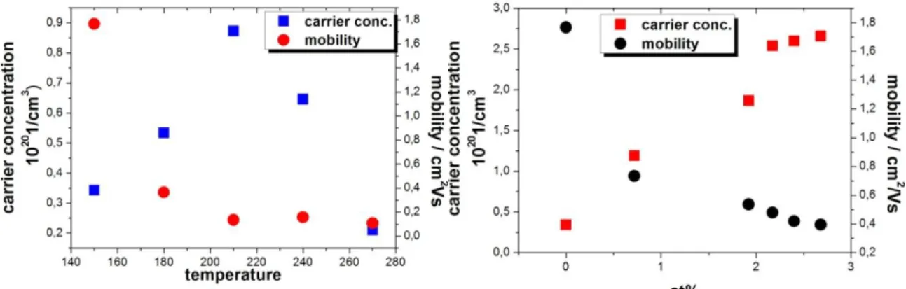
According to the available literature the resistivity of intrinsic ZnO decreases monotonically between 100°C and 200°C growth temperatures. Surprisingly, in this range both the electron mobility and the carrier concentration appear to decrease at the same time, although generally increasing concentration is associated with decreasing mobility. The reason for this opposite effect in ALD ZnO may be the consequence of the improved crystal structure of the layers obtained at elevated deposition temperature [2.2.22, 2.2.29-2.2.32] .
Schuisky et. al. [2.2.34] examined the film growth during ZnO deposition with in situ resistivity measurements with contacts fabricated on the substrate in Van der Pauw geometry, and measured the resistivity changes during layer deposition. They found that it monotonously decreased with the increasing thickness up to about 50 nanometre film thicknesses. Also, the resistivity varied cyclically between the deposition cycles. It increased at every diethyl-zinc exposure and decreased after every water pulse. This may be due to the difference of the surface conductance with different adsorbates chemisorbed on the surface. As a DEZ molecule is chemisorbed at the surface, due to Eq. 2.1. the surface OH groups are transformed into Zn-alkyl groups, then after the water exposure the original OH coverage returns. That is, the OH-terminated surface has a much lower resistivity than the ethyl-terminated one.
ALD grown ZnO films have a very low intrinsic resistivity of ~10-2 Ωcm, also depending on a number of deposition parameters. This low value is believed to be the result of the presence of Zn interstitials, oxygen vacancies and hydrogen
contamination [2.2.16-2.2.19]. This resistivity can be further reduced by two orders of magnitude at the most by Al doping [2.2.20, 2.2.23, 2.2.35-2.2.39].
Al doped ALD ZnO
The ALD grown ZnO can easily be doped with a number of materials, e.g. Al2O3, and multilayer structures can also easily be grown from these compounds. Composite thin films have long been the focus of research, as the refractive index, dielectric constant, lattice parameter and a number of other physical properties may be controlled by alloying two different materials. The composite material can also be fabricated as multilayers of the two constituents, which is quite straightforward with the ALD method. The doping and alloying of ZnO layers with Al with the ALD method has been examined by quite a few groups [2.2.20, 2.2.23, 2.2.35-2.2.39]. The doping of ZnO with Al by ALD occurs with inserting Al precursor pulses among the DEZ and the water pulses. The Al pulses are of course followed by water pulses, which raises the question if the Al is then built in as Al2O3, or the Al alone is placed as a substitutional dopant into the Zn location of the crystal. That is, is the resulting layer an alloy of the two oxides or an Al doped ZnO layer?
The growth of ZnO and Al2O3 layers is an interesting issue. The growth rate of ZnO is around 0.2 nm per cycle according to literature values, while that of Al2O3 is around 0.1 nm. Still, a multi-layer or an alloy of these two has much lower growth rates, as both materials have nucleation issues, and when the pulse sequences are changed, one has to nucleate on the other. Experiments have shown that after an Al2O3 pulse the growth rate of ZnO is much lower, and the same applies to the Al2O3 growth. The Al2O3 growth has a short nucleation period. It changes from 0.1 to 0.13 nm growth rate in 25 growth cycles. The ZnO on the other hand increases from 1.5 to 2 nm growth /cycle in 700 growth cycles. The surface chemistry of both materials is ruled by the hydroxyl coverage of the substrate. The hydroxyl coverage of amorphous Al2O3 is 0.94*1015/cm2, that of (100) ZnO is 1.06*1015/cm2, both defined at 177°C.
The DEZ molecule reacts in average with 1.37 and the TMA with 1.47 hydroxyl groups at the surface [2.2.37].
George et. al. [2.2.37] measured the Zn content of the deposited alloy layers, and found that it was way below the expected value. They found that for example in the case of 50% ZnO and Al2O3 ratio the growth rates of the two materials were way below the intrinsic values: 27% and 67% of the corresponding ZnO and Al2O3 values.
When the two materials have to nucleate on each other, the nucleation of ZnO lasts for about 6 cycles after each TMA pulse, and 2-3 TMA pulses are required after each DEZ pulse for the Al2O3 to nucleate. These could be the results of a smaller amount of surface reactive sites. But, as shown above, both the hydroxyl coverage and the reaction type of the two surfaces is similar, therefore the reduced growth cannot be a result of the lack of OH species. One explanation might be that the relative acidity of the two surfaces is different, and the following reaction may occur:
2.3.)ZnOH*+AlOH*→ZnOH2+…AlOH-*.
In which case the ZnOH2+…AlOH-* complex formation results in less reactive OH species left on the surface.
Besides the nucleation problems another effect decreases the growth of the ZnO- Al2O3 alloys and multilayers. In the ZnO concentration range of 75-85% even negative growth rates can be experienced, that is an etching for ZnO. During in-situ quartz crystal microbalance measurements it was found that the etching always occurred during the TMA exposure of the layer, when the thickness decreased as much as one deposition/cycle. The explanation for the phenomenon is the following surface reaction:
2.4.)ZnOH*+Al(CH3)3 →Al(OH)(CH3)*+Zn(CH3)2.
The loss of mass predicted by this agrees reasonably well with the experimental results.
The literature has reported an etching of metals in atomic layer deposition before as well, for example in the case of TaCl5 and Ta2O5 films, or Sr(thd)2 with the SrO surface, etc. ZnO is also etched by a CH4 plasma. In the case of the Al2O3 doping the CH4 from the TMA and the hydroxylated ZnO surface reaction abstracts a Zn and forms Zn(CH3)2. On the other hand the donating of CH3 groups from the Al to the Zn can also occur directly. The third etching effect can be the formation of ZnAl2O4
spinels.
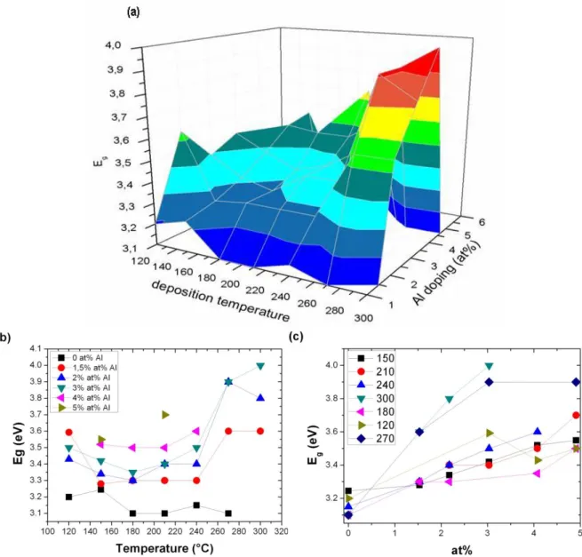
Many authors have examined the effect of the Al doping and the temperature on the resistivity of ZnO layers, but only one or the other, or just in a limited temperature or doping range. No comprehensive study has been conducted yet about the effectiveness of the doping at different temperatures.
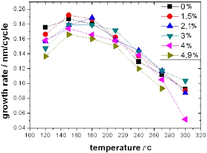
It was reported that the lowest resistivity could be achieved with Al content between 1 and 5 at%. At higher concentrations the mobility decreases, but the layers maintain their conductivity up to Al concentration as high as 10 at%. Between 10 and 16 at% the resistivity increases again, and small Al2O3 grains are formed in the layers. The crystallinity of the doped ZnO deteriorates, they may even become amorphous. Although it has been suggested that the doping efficiency may correlate with the ALD growth temperature [2.2.35, 2.2.38, 2.2.39], no detailed investigation was conducted on the subject so far.
Many groups have examined the effect of post annealing on the conductivity and the structural and morphological properties of the ALD deposited ZnO layers. It has been established that the post annealing results in a more uniform distribution of the Al doped sub-layers along the depth profile of the layers. However, the thermal treatment tends to increase the resistivity of the films. The most probable explanation is that the residual oxygen always present in every vacuum system diffuses into the layers and neutralises the intrinsic dopants. The oxygen vacancies quite obviously, but the hydrogen donors may also be engaged by the oxygen. If on the other hand the annealing was performed under some kind of capping layer an enhanced conductivity could be achieved [2.2.40-2.2.43].
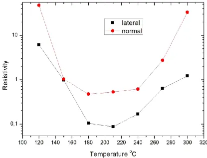
The effect of the Al doping on the crystallinity and the orientation of the layers has not been examined yet. The effect of grain boundaries in the conduction process, or whether the conductivity may be in connection with the orientation of the layers has not been examined either, despite the fact that it is known to have an effect on the resistivity of sputtered layers [2.2.25]. It has been reported in a number of works [2.2.22, 2.2.28, 2.2.29, 2.2.31, 2.2.32] that the orientation of the ZnO layers depends
on the deposition temperature. This implies that the columnar crystallites of the layers either stand normal to the surface, or lie parallel to it. This means completely different grain boundary conditions, and if the conduction is in connection with the grain boundaries, this must also have an effect on the resistivity as well.
2.3 CIGS solar cells
Cu(In,Ga)Se2 materials are one of the most promising members of the chalcopyrite family, due to their high absorption coefficients (105 cm-1), long term electrical and thermal stability and outstanding stability against photo-degradation. They have the highest efficiency among the thin film technologies [2.3.1.]. The most important chalcopyrite compounds for photovoltaic applications are Cu(In,Ga)(S,Se)2, which is an immensely complex system, of which we have a surprisingly low level of understanding compared to the achieved technological level. Most qualities (e.g.
morphology, electronic structure and band diagram) of this material have been experimentally set to achieve the best efficiency, while a complete understanding of them is still missing.
CIGS based thin film solar cells can be deposited on a number of substrates. Most commonly used is a glass sheet but recent attempts have been made to deposit chalcopyrite solar cells on flexible substrates. These efforts resulted in cells with efficiencies as high as 17.6% [2.3.2].
The components of CIGS solar cells
Thin film solar cells can be built up in superstrate or substrate configurations. In the case of a superstrate layout the deposition starts with a substrate, on which the transparent contact layer is deposited, followed by the buffer layer, the absorber, and finally the back contact. This method is the less common one, as it yields solar cells with lower efficiencies. The reason for this is the inter-diffusion of CdS and CIGS during absorber deposition [2.3.4].
The most widespread configuration is the substrate configuration shown in fig. 2.3.1.
Fig. 2.3.1 The cross section of the CIGS film deposited in substrate configuration [2.3.]
In the substrate based structure the back contact electrode of the cell is first deposited on the substrate. This is usually a Mo layer, a highly conductive material that can conveniently and highly reproducibly be deposited by sputtering. On the back electrode, the active layer, the p-type CIGS film is deposited. On top of this layer an n-type buffer layer is deposited, followed by the transparent conductive front contact, which is most generally Al doped ZnO prepared by sputtering [2.3.5].
The most commonly used substrate is soda lime glass, with a thickness usually between 1 mm and 3 mm. The choice of material is crucial: experiments have shown that the sodium content of the substrate material is indispensable. The Na diffusion from the substrate into the absorber layer increases the carrier concentration and also alters the structure of the layer: it yields a larger grain size and an overall better layer morphology. It increases the composition range tolerated by the structure, assists the selenization and changes the defect distribution by neutralizing deep level donors, thus increasing the p-type conductivity [2.3.6]. The Na diffusion into the absorber is independent of the qualities of the Mo layer.
The back contact is most commonly molybdenum, on which the active CIGS material grows uniformly, forming an ohmic contact. The qualities of the Mo layer can also greatly depend on the deposition parameters, and thus a number of the properties of the resulting cells can be tuned. Mo films deposited at a low Ar background pressure have low resistivities but possess compressive stress and a weak adhesion to the substrate. With the increasing pressure, the resistivity increases and a tensile stress appears. The layers deposited at high pressure have an excellent adhesion and at the same time smaller grains, but are also more porous than low pressure ones. Due to their morphology they offer more nucleation sites for the absorber layer, which ultimately results in a better absorber adhesion and smaller, less faceted absorber grains. To combine the good qualities of the different deposition methods Scofield et.
al. [2.3.7] developed a bilayer process with the deposition of a thin Mo layer at high Ar pressure immediately followed by a thicker one at low background pressure. This way it was possible to achieve low resistivity films with a good adhesion, which were then used in the best efficiency solar cells.
Between the active layer and the front electrode the buffer layer has a number of different roles. It is supposed to fit the lattices to each other and set the proper band offsets. It is also widely believed to prevent recombination at the interfaces. The buffer layer is usually CdS which offers a perfect n-type match to the p-type CIGS.
There are attempts to replace this material with others, because of the high toxicity of cadmium. Furthermore, as this film is deposited by chemical bath deposition it requires the interruption of the vacuum process. Intrinsic ZnO is one of the leading candidates for this purpose, but it has to cover the CIGS layer very uniformly, therefore special deposition methods are required. Atomic layer deposition promises to fulfil all these requirements [2.3.8].
The CIGS absorber layer
The most important chalcopyrite compounds as absorber layers for photovoltaic applications are Cu(In,Ga)(S,Se)2. By combining these components, a wide range of lattice constants and band-gaps may be achieved. The lattice constant of CIS
(CuInSe2) is 0.58 nm, its band gap is 1 eV, those of CGS (CuGaSe2) are 0.56 nm, and 1.7 eV. Thus the material qualities and the band gap of the absorber material may be tailored between these values even along the depth profile of the layer. The band gap corresponding to highest efficiencies achievable with a given method is 1.2 eV, which can be realized with a Ga/(Ga+In)=0.3 ratio. Above this ratio the quality of the films starts to decrease [2.3.9].
Although CIGS technology is not as sensitive to stoichiometry as Si based technology, still, the quality of the CIGS film depends largely on the exact composition of the layers. The CIGS material is doped p-type by native defects. The most important defect is the (2VCu,InCu) complex, which is a stable defect providing a shallow acceptor level. This means that a slightly Cu poor composition is actually advantageous, and the CIGS material needs to be deposited copper deficient.
Therefore the atomic ratio of the metals has to be between 0.88<Cu /(In+Ga)<0.95 and Ga/ (In+Ga)=0.3. Although a few percents of difference from this exact molecularity may still result in functioning layers, the films with various compositions differ in many qualities, most importantly in their performance. As mentioned before, the Na incorporation also increases the range in which the molecularity may change and still yield fairly high efficiency solar cells: The ratio of (In+Ga)/(In+Ga+Cu) may vary between 0.52 and 0.64 in the presence of Na [2.3.10].
Copper rich films have a larger grain size, caused by a segregation of CuSe at the grain boundaries, which has a low melting point and thus serves as a fluxing agent promoting the growth of large, closely packed crystallites. On the other hand, In rich layers have better electrical qualities. The bilayer process combines these advantages by depositing a Cu rich layer under a Cu poor one [2.3.11].
Manipulating the Ga content of the layer gives another possibility to engineer the qualities of the layer through its depth. Increasing the Ga/In ratio towards the depth of the layer results in a wider band gap near the back contact, which ultimately gives a higher open circuit voltage (Voc) and fill factor. At the same time it is crucial that the band gap is wide near the active region of the p-n junction, so that high-energy photons can still generate electron-hole pairs. The optimal band gap grading is defined by the optimum of these effects [2.3.12- 2.3.13].
Fig. 2.3.2. The band diagram of a CIGS solar cell [2.3.]
An interesting aspect of the details of the deposition is the sensitivity of the films to
their orientation. Not only the morphology but even defect formation depends largely on the crystallinity of the absorber layers. The most common orientations found in CIGS films are the (112) and (220/204). The (220/204) orientation has been observed as more prominent in the record efficiency absorber materials as it has a lower ratio of non-radiative recombination centres. This crystallinity can be achieved with a Se overpressure, or a higher Se flux, with the substrate type Na and Cu content also playing a part in the resulting orientation [2.3.14, 2.3.15].
The highest reported conversion efficiency for CIGS solar cells is beyond 20% for laboratory scale cells [2.3.16]. This result has been produced by an inline co- deposition method, where all the compounds are co-evaporated from individual sources. This is the technique promising the best quality cells, but also the most complex one possible, in which the precise control of all the parameters e.g.
substrate velocity, temperature and composition profiles is necessary.
Deposition methods
The co-deposition method is often performed as a sequence of deposition processes, where the concentration of the components varies with time. During evaporation the Se is always in excess, but the Ga/In ratio can be changed during the process thus tailoring the band-gap throughout the depth of the layer. Changing the copper content also changes the growth kinetics of the film. The bilayer process unites the advantages of the Cu poor layers on the electronic structure and the Cu rich layers on the morphology. The deposition starts with a relatively Cu rich layer, which gives larger grain size and an overall better film morphology, and ends with a Cu poor layer, which ensures the optimal electrical qualities. The inverted process is the same reversed. The three-stage method begins with the co-evaporation of In, Ga and Se, which results in a very smooth base layer. This is followed by an exposure to Cu and Se in the second stage, until a Cu-rich composition is achieved, and then additional In, Ga and Se are supplied to adjust the precise film composition and give a smooth layer surface [2.3.17].
Besides co-evaporation there is a number of other processes to fabricate CIGS films such as selenization of the precursors with Se vapour [2.3.18-2.3.34], H2Se or diethylselenide [2.3.33,2.3.35], the rapid thermal processing of co-deposited or stacked multi-layer precursors [2.3.36], spray pyrolisis [2.3.37], flash evaporation [2.3.38], RF sputtering [2.3.39], electrodeposition [2.3.40], chemical bath deposition [2.3.41], etc.
The two step method for CIGS preparation
The two-step method means the deposition and post-selenization of the metallic components, and is a promising method for low cost, large scale manufacturing of solar cells. It is fairly simple, and does not require expensive apparatus or a very precise control of the parameters, as the thus created layers are not as sensitive to the growth parameters as the ones grown with one-step methods. Still fairly high efficiencies can be achieved with this approach. Films prepared with this method have efficiencies smaller with a few percents than the record ones on the laboratory scale, but once the one major difficulty of scaling up has been avoided, these
differences are significantly smaller. Siemens solar uses this preparation method, and they have achieved modules with 15% efficiency [2.3.18].
Selenization can be carried out on the copper-indium-gallium layer thus creating CIGS material, or on the other hand the quality of the already deposited CIGS material can be largely improved by a selenization with simultaneous annealing. A post-deposition thermal treatment in Se atmosphere improves the film stoichiometry and the structure [2.3.26].
Selenization is usually achieved by the use of Se vapour, or H2Se. The latter is highly toxic, therefore its application raises environmental and health concerns. It is usually stored in high pressure cylinders, so its handling is somewhat complicated.
There have also been successful recent attempts of selenization with diethyl- selenide [2.3.26, 2.3.27].
Paradoxically, the Se content of the layers is not always increased by selenization.
The reported decrease of the Se content during selenization due to the outdiffusion of Se can be avoided by a very rapid ramp up [2.3.19].
The metals can also be deposited on the substrates by a number of methods, evaporation and sputtering being perhaps the most common. A paste coating of the metallic components [2.3.20] or a metallic ink coating with a post selenization [2.3.21] are two of the unconventional methods that provide a simple non-vacuum process for absorber preparation, although the device efficiencies do not exceed 10
% at the moment. The problem most often associated with these methods is that the paste quality seems to be poor. The homogeneous mixing of the different metals within the powder and the milling of sufficiently small particles without contaminating the materials has yet to be solved. Current efforts are aimed at dissolving nano-sized particles in the fluxing agents [2.3.22] or the milling of alloys of Cu, Ga and In, which are more brittle, therefore a more homogeneous powder with smaller particle size can be made from them [2.3.21].
There have been a number of studies on the processes that take place during the selenization of Cu, In and Ga, but no full description has been given yet. Most studies examine the process by ex-situ methods [2.3.22], but there have been certain attempts for the in situ characterization of the CIGS formation. Liu et al [2.3.34] used in-situ electrical resistance measurement, while Kim et al. used time-resolved high temperature XRD [2.3.35]. There is no detailed analysis of the diffusion of Se in the metallic components, and the influence of a number of parameters such as time, pressure and heating method on the diffusion is not yet understood. However, from the work of Kim et. al., it appears that the formation of both CIS and CIGS materials is a one dimensional diffusion controlled process with a nucleation and a subsequent growth step. The growth kinetics consists of the growth of a CIS or CIGS layer on the surface of the material, which then limits the diffusion speed. The process was estimated both with the Avrami and the parabolic rate growth model and an activation energy of 100-130 kJ/mol was found for the CuInSe2 formation.
Several studies address the chemical reactions that take place in the process. It has been established that if the temperature during selenization is reached through ramp annealing, the formation of the binary and ternary composites follow a certain
![Fig. 2.3.1 The cross section of the CIGS film deposited in substrate configuration [2.3.]](https://thumb-eu.123doks.com/thumbv2/9dokorg/1309420.105343/23.892.220.679.718.1048/fig-cross-section-cigs-film-deposited-substrate-configuration.webp)