Research Article
Modeling of Label-Free Optical Waveguide Biosensors with Surfaces Covered Partially by Vertically Homogeneous and Inhomogeneous Films
Balint Kovacs and Robert Horvath
Nanobiosensorics Laboratory, MTA EK MFA, Budapest, Hungary
Correspondence should be addressed to Robert Horvath; r74horvath@gmail.com Received 19 October 2018; Accepted 14 January 2019; Published 31 March 2019
Academic Editor: Stephen James
Copyright © 2019 Balint Kovacs and Robert Horvath. This is an open access article distributed under the Creative Commons Attribution License, which permits unrestricted use, distribution, and reproduction in any medium, provided the original work is properly cited.
Optical Waveguide Lightmode Spectroscopy (OWLS) is widely applied to monitor protein adsorption, polymer self-assembly, and living cells on the surface of the sensor in a label-free manner. Typically, to determine the optogeometrical parameters of the analyte layer (adlayer), the homogeneous and isotropic thin adlayer model is used to analyze the recorded OWLS data. However, in most practical situations, the analyte layer is neither homogeneous nor isotropic. Therefore, the measurement with two waveguide modes and the applied model cannot supply enough information about the parameters of the possible adlayer inhomogeneity and anisotropy. Only the so-called quasihomogeneous adlayer refractive index, layer thickness, and surface mass can be determined.
In the present work, we construct an inhomogeneous adlayer model. In our model, the adlayer covers the waveguide surface only partially and it has a given refractive index profile perpendicular to the surface of the sensor. Using analytical and numerical model calculations, the step-index and exponential refractive index profiles are investigated with varying surface coverages from 0 to 100%. The relevant equations are summarized and three typically employed waveguide sensor structures are studied in detail. We predict the errors in the calculated optogeometrical parameters of the adlayer by simulating the OWLS measurement on an assumed inhomogeneous adlayer. We found that the surface coverage has negligible influence on the calculated refractive index belowfilm thicknesses of 5 nm; the calculated refractive index is close to the refractive index of the adlayer islands. But the determined quasihomogeneous adlayer refractive index and surface mass are always underrated; the calculated quasihomogeneous thickness is heavily influenced by the surface coverage. Depending on the refractive index profile, waveguide geometry, and surface coverage, the thickness obtained from the homogeneous and isotropic modeling can even take negative and largely overestimated values, too. Therefore, experimentally obtained unrealistic adlayer values, which were dismissed previously, might be important indicators of layer structure.
1. Introduction
Evanescent field-based optical techniques are popular in surface sensitive chemicals and biosensors. The intensity of this evanescent wave is the highest at the sensing surface and is exponentially decaying in the media above the sen- sor. Typical examples of these techniques are the surface plasmon resonance [1–3] and planar optical waveguide- based techniques [4–9]. Usually, the latter have higher sensitivities, especially when combined with optical inter- ferometry [10]. These techniques can also be combined with absorption spectroscopy [11–13]. Nowadays, these
methods are well established and also available in high- throughput format [8, 9, 14–16].
Among waveguide-based sensors, Optical Waveguide Lightmode Spectroscopy (OWLS) is one of the oldest and most popular methods, realized in reliable commercial devices [6]. The basic sensing effect was discovered and theoretically explained by Tiefenthaler and Lukosz [17].
They realized that the resonant angle of the coupled light into a grating coupled planar optical waveguide shifts upon changing the optical parameters of the media covering the grating area [17]. The technique is completely label-free and has been used so far for gas sensing [18], monitoring of
Volume 2019, Article ID 1762450, 11 pages https://doi.org/10.1155/2019/1762450
protein adsorption [6], live cell adhesion [19], examining protein-DNA interaction [20], lipid bilayers [21], polyelec- trolyte multilayers [22], and nanoparticle self-assembly [23].
One drawback of the traditional OWLS technique is that it does not have imaging capabilities, like imaging ellipsome- try, imaging SPR [15, 16], or the recently introduced reso- nant waveguide gratings [8, 14, 23]. However, an important advantage of OWLS is that it can measure the effective refrac- tive indices of two optical resonances, corresponding to the zeroth order transverse electric (TE) and transverse magnetic (TM) modes. By applying these two independent quantities, the thickness and refractive index of the deposited adlayer can be calculated. Typically, the homogeneous and isotro- pic thin adlayer model is used to evaluate the OWLS data.
But, in most applications, the analyte layer is neither homogeneous nor isotropic. Still, by employing the homoge- neous and isotropic thin adlayer model, even if it predicts highly unrealistic values, important information about optical anisotropy in the analyte layer can be obtained [24].
In the present work, we investigate the OWLS signals when the adlayer covers the waveguide surface only partially and the adlayer refractive index is inhomogeneous perpen- dicular to the surface of the sensor. Using analytical and numerical model calculations, the step-index and exponen- tial refractive index profiles are investigated with varying
surface coverages from 0 to 100%. The relevant equations are summarized and three different typically employed waveguide sensor structures are studied in detail.
2. Modeled Structures and Methods
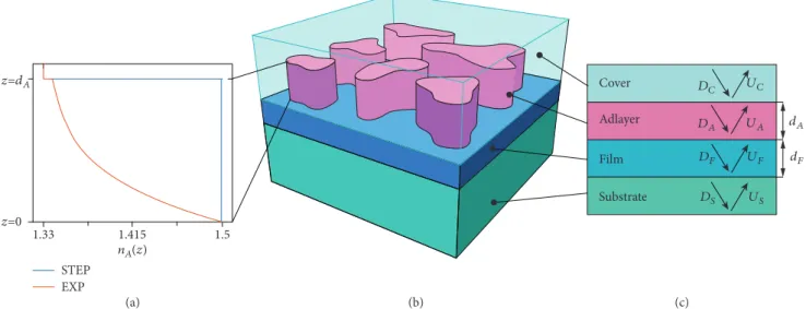
2.1. The Modeled Waveguide and Adlayer Structures and the Applied Algorithms. The structure of the waveguide sensor and the investigated adlayer models is visualized in Figure 1. The waveguides consist of an electromagnetically half-infinite thick substrate with refractive index nS, cov- ered by a waveguide film with refractive index nF and thickness dF. In this paper, the monitored adlayer covers only partially the waveguide film with θ surface coverage, and it has dA layer thickness and nA z refractive index, which can depend on the verticalzdistance from the wave- guide layer. The media above the adlayer is an aqueous solution with refractive index nC= 1 33.
During the model calculations, the thickness of the adlayer was varied between 0 and 500 nm. The adlayer was considered horizontally inhomogeneous with θ surface coverage values from 0% to 100%. We modeled two types of refractive index distributions by dividing the adlyer covered areas into 150 sub- layers in the vertical direction withnMAXA = 1 5, the exponential and step-index refractive index profiles (see Figure 1(a)):
z=dA DC
DA DF DS US
UF UA UC
dA dF
z=0
nA(z)
1.33 1.415
(a) (b) (c)
Cover Adlayer Film Substrate 1.5
STEP EXP
Figure1: The structure of the modeled OWLS waveguide chips with inhomogeneous adlayer. The modeled multilayered assembly consists of 4 layers: substrate, waveguidefilm, adlayer, and cover (see inset c). The adlayer covers the waveguidefilm surface in a certain percent (see inset b) and it hasnA z vertical refractive index distribution: step-index and exponential distribution (see inset a). This vertical distribution is realized in our model calculations by dividing the adlayer into 150 sublayers (not shown infigure) which has the appropriate refractive index of the selected distribution. These layers are implemented in the transfer matrix method whereU andDare the amplitudes of the upward and downward propagating electromagnetic waves (see inset c and equation (4)).
Step‐index profile 0≤z<dA⟶nA z =nMAXA , dA≤z⟶nA z =nC,
Exponential profile 0≤z<dA⟶nA z =nC+ nMAXA −nC ⋅e−3/dA⋅z, dA≤z⟶nA z =nC
1
The step-index profile is a widely applied model for a compact protein layer [4, 25] and the exponential profile is reported to characterize adlayers of flexible polymers with attractive surface-polymer interaction [26–28]. Gaussian, linear, and power-law distributions could be also treated in a straightforward manner [29, 30].
The optogeometrical parameters of the planar optical waveguide structures treated here are summarized in Table 1. The OW2400 and Ta2O5 are monomode wave- guide sensors, which were designed to monitor molecular scale adlayers with mode penetration depths of around 80-110 nm. In contrast, the modes of the “Reverse” wave- guide design have larger penetration depths into the aqueous cover media. This design is more suitable to monitor living cells [31].
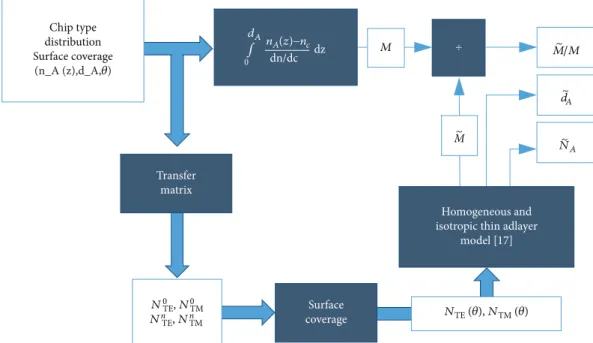
The model calculations performed in the present study are schematically overviewed in Figure 2 with the previously modeled waveguide structure (chip type) and the horizon- tally (surface coverage) and vertically (adlayer refractive index profiles) inhomogeneous analyte layer. The aim of the algorithm is identifying the possible errors in the outputs of the widely used isotropic and homogeneous thin adlayer model by simply comparing the input parameters and the obtained quasihomogeneous nA refractive index, dA layer thickness, and M surface mass, which all can be obtained from the examined homogeneous and isotropic model (see details later). Note that the effect of the horizontal inhomoge- neity (surface coverage) on the measurement results is also in the focus of this paper.
2.1.1. Input Parameters.The input parameters of the algo- rithm are nMAXA = 1 5 refractive index, nA z refractive index distribution of the adlayer, type of sensor chip, sur- face coverage, and thickness of the adlayer, which varied between 0 and 500 nm. The surface coverage is labeled by θ and it can take values between 0 and 1; the latter means 100% coverage.
2.1.2. Calculating the Effective Refractive Indices Taking the Surface Coverage into Account. In order to simulate the isotropic and homogeneous thin adlayer model, NTE θ and NTM θ effective refractive indices of the modeled structure are needed. The effective refractive index is defined as
N=β
k, 2
where k is the vacuum wave number and β is the propa- gation constant. The effective refractive index values depend on the covering adlayer. Therefore, two indepen- dent calculations are needed to obtainN0 effective indices for the uncovered areas and Nn effective refractive index for the adlayer covered areas.
In short, the transmission and reflection coefficients of the waves of the TE and TM modes at each boundary are
determined by using the Maxwell’s equations and the boundary conditions [32].
tTE= 2 ·k1z k1z+k2z, rTE=k1z−k2z
k1z+k2z, tTM= 2 ·ε2·k1z
ε2·k1z + ε1·k2z , rTM= ε2·k1z − ε1·k2z
ε2·k1z + ε1·k2z
3
(For notations, see reference [32].) Using these coefficients by applying the transfer matrix equations, the following simple formula connects the wave ampli- tudes in the two layers, which were divided by a given boundary.
1
ti · 1 ri
ri 1 · Ui·ej·kiz·di
Di·e−j·kiz·di = Ui+1·ej·ki+1,z·di Di+1·e−j·ki+1,z·di ,
4
where i is the layer index and j is the imaginary unit and U and Dare the amplitudes of the upward and downward propagating electromagnetic waves in the indexed media (see Figure 1(c)).
For the whole structure, 2n+ 3 parameters and 2n equations are obtained—where n equals to the number of boundaries. Since we are looking for the solutions of the bounded modes,DC and US are equal to 0 and one of the amplitudes can be fixed to 1, so the above set of equations can be solved. This results in N0TE,N0TM for the uncovered areas andNnTE,NnTMfor the adlayer covered areas. Therefore, the effective refractive index differences at the covered and uncovered areas for TE and TM modes can be easily calculated:
ΔNTE=NnTE−N0TE, 5
ΔNTM=NnTM−N0TM 6 Table1: The structural parameters of the modeled planar optical waveguide sensors.
nF nS dF
OW2400 1.77 1.52 200 nm
Ta2O5 2.12 1.52 150 nm
Reverse 1.575 1.2 150 nm
The effective refractive indices of the modes with θ surface coverage were calculated by applying the following equations [33]:
NTE θ =N0TE+θ·ΔNTE, 7 NTM θ =N0TM+θ·ΔNTM 8 2.1.3. Simulating the Homogeneous and Isotropic Thin Adlayer Model. Then, the effective refractive indices from equations (7) and (8) were substituted into the homoge- neous and isotropic thin adlayer model [17], resulting in the numerical values of nA, dA, and M, where M= dA· nA−nC / dn/dc , and in this paper, nA, dA, and M are referred as the adlayer parameters that resulted from the quasihomogeneous analysis.
On the other hand, the surface mass of the adlayer with a certain θ surface coverage was also calculated from the following integral, using the refractive index distribution of the adlayer:
M=
dA 0
nA z −nC
dn/dc dz, 9
wheredn/dcis the so-called refractive index increment of the protein or polymer solution used to deposit the adlayer [4, 6].
At the end of these calculations, the results are the quasihomogeneous optogeometrical parameters and the ratio of the two surface masses:nA,dA, andM/M.
2.1.4. Further Analytical Calculations Modeling the Adlayers.
Moreover, we have calculated an averaged adlayer refractive index and thickness based on the following well-known equations, too [29, 30].
nA=
dA
0 n z · n z −nC dz
dA
0 n z −nC dz , dA=
dA
0 n z −nC dz nA−nC
10
The above formulae do not take the possible inhomo- geneities in adlayer refractive index parallel to the surface (surface coverage) into consideration. Considering the surface coverage, the following equation was applied:
n z =θ·nA z + 1−θ ·nC 11 After straightforward calculations, we obtained
nA θ =
dA
0 θ·nA z + 1−θ ·nC ∗ nA z −nC dz
dA
0 nA z −nCdz ,
12
dA θ =θ·
dA
0 nA z −nC dz
nA−nC 13
Chip type distribution Surface coverage (n_A (z),d_A,𝜃)
Transfer matrix
M ÷ M~
/M
M~
d~
A
NA
Surface coverage
Homogeneous and isotropic thin adlayer
model [17]
NTE (𝜃), NTM (𝜃) N0TE, N0TM
NnTE, NnTM
∫ dA
0 ndn/dcA(z)−ncdz
Figure2: The structure of the developed MATLAB algorithm. The input parameters are the parameters of the chip structure and the parameters of the modeled adlayer: the refractive index, the layer thickness, the surface coverage, and the vertical refractive index distribution. The algorithm has two main paths. In the upper one, the real surface mass is calculated with an integral. In the other path, the effective refractive indices were calculated from the input parameters, then these values were applied in the homogeneous and isotropic model resulting in quasihomogeneous surface mass, adlayer thickness, and refractive index. The output parameters of the algorithm are the quasihomogeneous refractive index, the layer thickness, and the ratio of the obtained masses.
3. Results and Discussions
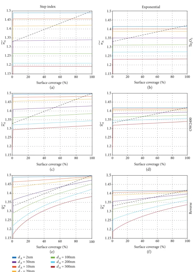
3.1. The Quasihomogeneous Adlayer Refractive Index and Thickness with Varied Surface Coverage.The results obtained for the step-index and exponential profiles are summarized in Figures 3–6. Previous calculations performed for compact adlayers (100% coverage) concluded that by increasing dA, the quasihomogeneousnAunderrates the refractive index of the adlayer (nA= 1 5) more and more [32]. This effect can also be clearly seen in Figure 3 for both distributions.
Here, the effect of surface coverage on nA is shown. If dA is increased, nA is underrated and it even takes values below 1.33 above 100 nm adlayer thicknesses, depending on the actual waveguide design and surface coverage (see Figure 3).
Interestingly, the surface coverage has almost no influ- ence on the obtainednAvalue in the case of the Ta2O5and OW2400 waveguide designs. The dependence of surface coverage somehow appears in case of the reverse waveguide design only. With increasing surface coverage,nAis increas- ing too. However, for very thin adlayers (below 5 nm), this effect is completely missing even for the reverse waveguide design. But, this type of behavior can be elegantly predicted by analytical calculations. Simply, we apply the linearized mode equations for thin adlayers [17] and equations (7) and (8). The following set of equations can be obtained after straightforward calculations. From the equations for TE mode, we obtain
nA−nC ·dA=θ· nA−nC ·dA, 14 and from the equations for TM mode, we get
NTM nC +NTM
nA −1 · nA−nC ·dA
=θ· NTM nC +NTM
nA −1 · nA−nC ·dA 15
By solving equations (14) and (15), one can calculate the quasi-isotropic thickness and refractive index of the adlayer:
nA=nA, dA=θ·dA
16
Therefore, for thin adlayers, the quasihomogeneous adlayer refractive index equals the refractive index of the modeled adlayer islands, independent of the surface coverage. The quasihomogeneous adlayer thickness line- arly depends on the surface coverage.
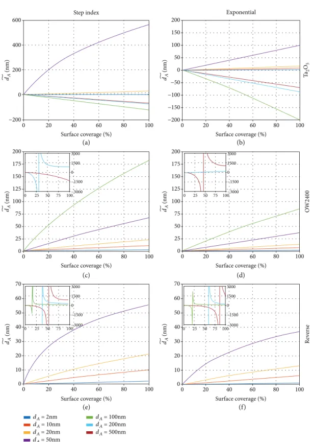
It is also important to note that whennA is below nC, negativedAvalues were obtained in all cases. This is the rea- son why there are singularities in the“surface coverage-dA” curves (see Figure 4). When the value ofnAexceeds the value ofnC, the value ofdAchanges from negative to positive. It is important to note that the surface coverage has negligible influence on the obtainednAvalue for the Ta2O5chip. That
is why we hardly get any singularities in this case. These singularities are more frequent for the OW2400 and the reverse waveguide designs because the effect of the surface coverage is more specified for the OW2400 and the reverse optical waveguide geometry.
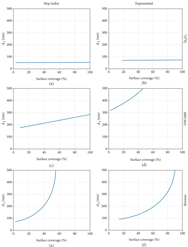
3.2. Conditions of Singularity in the Quasihomogeneous Adlayer Thickness.As pointed out, whennAhas values below nC, negative dA values were obtained in all cases. When nA=nC, a singularity appears in the “surface coverage-dA” graphs (see insets in Figure 4). The exact appearance of these singularities is plotted in Figure 5. For example, using the reverse chip in case of an adlayer film with dA= 200 nm and step-index distribution, its quasihomogeneous nA has the value ofnCat around 40% surface coverage. At that exact point,dAvalue changes its sign, a singularity appears.
For simplicity, in Figure 5, the lines mark those condi- tions whendA/dAvalue exceeds 20. The singularity is appear- ing only for larger thicknesses in the case of the reverse waveguide design. It is also important to note that the appearance of the singularity when the surface coverages are tuned is most specified for the reverse waveguide design.
Therefore, the reverse waveguide design is worth investi- gating with varying the surface coverages.
It is important to emphasize that the negative adlayer thickness has no physical meaning, as it originates from the application of a wrong model. But, for a complicated adlayer, which is characterized by more than two independent parameters, the two independent modes (TE, TM) and the isotropic and homogeneous adlayer model, which are applied in OWLS experiments, do not give enough independent equations to calculate all of the parameters of the adlayer.
Based on the presented results, however, the properties of the complicated adlayer can be deduced in some circum- stances from the nonphysical adlayer parameters. For example, if the Ta2O5sensor chip is used and negative quasi- homogeneous adlayer thicknesses are obtained, it is a clear indication that the adlayer has a step-index profile and its thickness is larger than 50 nm, or it has an exponential profile with a thickness above 80 nm. Importantly, the calculations also show that the surface coverage has practically no role in modifying these parameters (see Figures 5(a) and 5(b)).
Another example is the reverse chip with negative quasiho- mogeneous adlayer thickness with step-index distribution.
In this case, one can state that the surface coverage is less than 60% (see Figure 5(e)). Similar statements can be made for the other two chip types, too. This type of analysis can also be especially useful when the deposition of the adlayer is followed in real time and the surface coverage is continu- ously increasing or the surface coverage is constant, but the thickness is increasing (protein aggregation [34], polyelectro- lyte layer deposition [26, 27, 35, 36]).
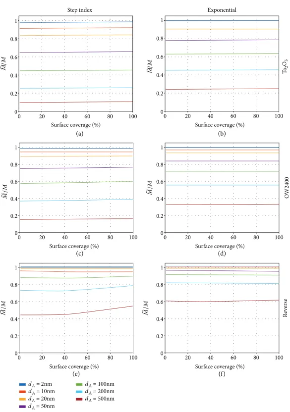
3.3. The Errors in Adlayer Mass with Varied Surface Coverage. In Figure 6, we investigate the errors introduced in the obtained mass by applying the quasi-isotropic adlayer model for partially covered surfaces. By increasingdA,M/M ratio deviates from the value 1 more and more, and the
quasihomogeneous analysis underrates the mass in all cases. It is important to emphasize that the surface cover- age has negligible influence, expect for the reverse geom- etry. Using the reverse chip in the case of an adlayer with
dA> 100 nm and step-index distribution, the M/M ratio curves have an arc. In that case with dA= 500 nm, the M/M ratio has ~0.45 and ~0.55 values at 0% and 100%
surface coverages.
1.5
Step index 1.45
1.4
1.3 1.25 1.2 1.15
0 20 40
Surface coverage (%)
(a) (b)
(c) (d)
(e) (f)
1.35 nA
60 80 100
Exponential
Ta2O5
1.5 1.45 1.4 1.35 1.3 1.25 1.2
1.150 20 40
Surface coverage (%)
60 80 100
nA
1.5 1.45 1.4 1.35 1.3 1.25 1.2
1.150 20 40
Surface coverage (%)
60 80 100
nA OW2400
1.5 1.45 1.4 1.35 1.3 1.25 1.2
1.150 20 40
Surface coverage (%)
60 80 100
nA
1.5 1.45 1.4 1.35 1.3 1.25 1.2
1.150 20 40
Surface coverage (%)
60 80 100
nA
1.5 1.45 1.4 1.35 1.3 1.25 1.2
1.150 20 40
Surface coverage (%)
60 80 100
nA Reverse
dA = 100nm
dA = 20nm
dA = 200nm dA = 2nm
dA = 50nm
dA = 10nm dA = 500nm
Figure3: The quasihomogeneous adlayer refractive index in the function of surface coverage for seven different adlayerfilm thicknesses. The dashed line represents the average value of the refractive index,nA θ, calculated from equation (12).
4. Conclusions
In the present work, we investigated the OWLS signals when the adlayer covers the waveguide surface only partially and
the adlayer refractive index is inhomogeneous perpendicular to the surface of the sensor. Using analytical and numerical model calculations, the step-index and exponential refractive index profiles were investigated by varying surface coverages
100 Surface coverage (%)
Step index
−200 0 200 400 600
80 60 40 20 0
dA (nm)
Exponential
Surface coverage (%)
(a) (b)
(c) (d)
(e) (f)
−200
−150
−100
−50 0 50 100 150 200
100 80 60 40 20 0
Ta2O5
dA (nm)
Surface coverage (%) 0
25 50 75 100 125
0 25 50 75 100−3000
−1500 0 1500 3000
150 175 200
100 80
60 40 20 0
dA (nm)
Surface coverage (%) 0
25 50 75 100 125 150 175 200
100 80 60 40 20 0
0 25 50 75 100−3000
−1500 0 1500 3000
OW2400
dA (nm)
Surface coverage (%)
0 25 50 75 100−3000
−1500 0 1500 3000
0 10 20 30 40 50 60 70
100 80
60 40 20 0
dA (nm)
Surface coverage (%)
0 25 50 75 100−3000
−1500 0 1500 3000
0 10 20 30 40 50 60 70
100
Reverse
80 60 40 20 0 dA (nm)
dA = 100nm dA = 20nm
dA = 200nm dA = 2nm
dA = 50nm dA = 10nm
dA = 500nm
Figure4: The quasihomogeneous adlayerfilm thickness in function of the surface coverage for seven adlayerfilm thicknesses. For thicker layer thicknesses—100 nm, 200 nm, and 500 nm—overrated values and singularities appeared in case of the OW2400 and the reverse chip.
The singularities are shown in the insets.
from 0 to 100%. The relevant equations were summarized and three different typically applied waveguide sensor struc- tures were studied in detail. We concluded that the surface coverage has negligible influence on the obtained quasiho- mogeneous adlayer refractive index for thin adlayers; the obtained index equals the refractive index of the adlayer islands. A simple analytical calculation supported thefind- ing of the numerical simulations. The quasihomogeneous
adlayer refractive index is always underrated for thicker adlayers, independent of surface coverage, waveguide sensor type, and refractive index profile. In special cases, the quasi- homogeneous refractive index of the adlayer can be equal to the refractive index of the cover media. In this case, a sin- gularity appears in the quasihomogeneous thickness. The obtained thickness can also be negative around the singula- rity. The conditions when the singularity appears were
500 400 300 200 100 0
0 20 40
Surface coverage (%)
60 80 100
Step index
dA (nm)
500 400 300 200 100 0
0 20 40
Surface coverage (%)
(a) (b)
(c) (d)
(e) (f)
Exponential
dA (nm)
60 80 100
Ta2O5
500 400 300 200 100 0
0 20 40
Surface coverage (%)
60 80 100
dA (nm)
500 400 300 200 100 0
0 20 40
Surface coverage (%)
60 80 100
100
OW2400
dA (nm)
500 400 300 200 100 0
0 20 40
Surface coverage (%) dA (nm)
60 80 100
500 400 300 200 100
00 20 40
Surface coverage (%) dA (nm)
60 80
Reverse
Figure5: The lines of the adlayer thickness-surface coverage pairs where the singularities appear.
analyzed in detail. This behavior is very similar to what was obtained for positively birefringent adlayers [24]. Therefore, our work is a strong evidence that overestimated quasihomo- geneous adlayer refractive index cannot originate from par- tial coverage and vertically exponential refractive index profile. In this case, the deposited adlayer is most probably negatively birefringent [24]. Note, in a recent study, an
unrealistically large 2.1 quasihomogeneous adlayer refractive index was measured for polymer films [37]. Moreover, we found a very strong dependence of the measured quasihomo- geneous adlayer refractive index on the surface coverage when the reverse waveguide design was employed. Therefore, in experiments where micron scale adlayer islands are formed, we suggest to use the reverse waveguide design. In
1 0.8 0.6 0.4 0.2
00 20 40 60 80 100
Step index
Surface coverage (%) M~ /M
1 0.8 0.6 0.4 0.2
00 20 40 60 80 100
Exponential
Surface coverage (%)
(a) (b)
M~/M Ta2O5
1 0.8 0.6 0.4 0.2
00 20 40 60 80 100
Surface coverage (%) M~ /M
1 0.8 0.6 0.4 0.2
00 20 40 60 80 100
Surface coverage (%)
(c) (d)
(e) (f)
OW2400
M~ /M
1 0.8 0.6 0.4 0.2
00 20 40 60 80 100
Surface coverage (%)
M~ /M Reverse
1 0.8 0.6 0.4 0.2
00 20 40 60 80 100
Surface coverage (%) M~ /M
dA = 20nm dA = 2nm
dA = 50nm dA = 10nm
dA = 100nm dA = 200nm dA = 500nm
Figure6: The ratio of the obtained masses in the function of the surface coverage for seven different adlayerfilm thicknesses.
summary, our work supplies important additional informa- tion for analyzing OWLS data, especially in those cases when the measured optogeometrical parameters of the adlayer were considered incorrect and not acceptable in previous experiments.
Data Availability
The parameters of the employed sensor structures and the modeled inhomogeneous analyte layer used to support the findings of this study are included within the article.
Conflicts of Interest
We confirm that the publication does not lead to any conflict of interest.
Acknowledgments
This work was supported by the Lendület Program of the Hungarian Academy of Sciences and by the ERC_HU, KH_17 Programs of the Nemzeti Kutatási, Fejlesztési és Innovációs Hivatal.
References
[1] M. Piliarik and J. Homola,“Surface plasmon resonance (SPR) sensors: approaching their limits?,” Optics Express, vol. 17, no. 19, pp. 16505–16517, 2009.
[2] J. Homola, “Surface plasmon resonance sensors for detec- tion of chemical and biological species,” Chemical Reviews, vol. 108, no. 2, pp. 462–493, 2008.
[3] J. Homola,“Present and future of surface plasmon resonance biosensors,”Analytical and Bioanalytical Chemistry, vol. 377, no. 3, pp. 528–539, 2003.
[4] J. Vörös, J. J. Ramsden, G. Csúcs et al.,“Optical grating coupler biosensors,”Biomaterials, vol. 23, no. 17, pp. 3699–3710, 2002.
[5] J. J. Ramsden, “Optical biosensors,” Journal of Molecular Recognition, vol. 10, no. 3, pp. 109–120, 1997.
[6] N. Orgovan, D. Patko, C. Hos et al., “Sample handling in surface sensitive chemical and biological sensing: a practical review of basic fluidics and analyte transport,” Advances in Colloid and Interface Science, vol. 211, pp. 1–16, 2014.
[7] Y. Fang, A. M. Ferrie, N. H. Fontaine, and P. K. Yuen,
“Characteristics of dynamic mass redistribution of epidermal growth factor receptor signaling in living cells measured with label-free optical biosensors,” Analytical Chemistry, vol. 77, no. 17, pp. 5720–5725, 2005.
[8] Y. Fang, A. M. Ferrie, N. H. Fontaine, J. Mauro, and J. Balakrishnan,“Resonant waveguide grating biosensor for living cell sensing,” Biophysical Journal, vol. 91, no. 5, pp. 1925–1940, 2006.
[9] Y. Fang,“Label-free cell-based assays with optical biosensors in drug discovery,”Assay and Drug Development Technologies, vol. 4, no. 5, pp. 583–595, 2006.
[10] D. Patko, K. Cottier, A. Hamori, and R. Horvath,“Single beam grating coupled interferometry: high resolution miniaturized label-free sensor for plate based parallel screening,” Optics Express, vol. 20, no. 21, pp. 23162–23173, 2012.
[11] R. Gupta and N. J. Goddard, “Broadband absorption spec- troscopy for rapid pH measurement in small volumes using
an integrated porous waveguide,” Analyst, vol. 142, no. 1, pp. 169–176, 2017.
[12] R. Gupta and N. J. Goddard,“Optical waveguide for common path simultaneous refractive index and broadband absorption measurements in small volumes,” Sensors and Actuators B:
Chemical, vol. 237, pp. 1066–1075, 2016.
[13] R. Gupta and N. J. Goddard,“A proof-of-principle study for performing enzyme bioassays using substrates immobilized in a leaky optical waveguide,” Sensors and Actuators B:
Chemical, vol. 244, pp. 549–558, 2017.
[14] N. Orgovan, B. Kovacs, E. Farkas et al., “Bulk and surface sensitivity of a resonant waveguide grating imager,”Applied Physics Letters, vol. 104, no. 8, article 083506, 2014.
[15] L. Simon, G. Lautner, and R. E. Gyurcsányi,“Reliable micro- spotting methodology for peptide-nucleic acid layers with high hybridization efficiency on gold SPR imaging chips,”Analyti- cal Methods, vol. 7, no. 15, pp. 6077–6082, 2015.
[16] G. Lautner, Z. Balogh, V. Bardóczy, T. Mészáros, and R. E.
Gyurcsányi,“Aptamer-based biochips for label-free detection of plant virus coat proteins by SPR imaging,” Analyst, vol. 135, no. 5, pp. 918–926, 2010.
[17] K. Tiefenthaler and W. Lukosz,“Sensitivity of grating couplers as integrated-optical chemical sensors,”Journal of the Optical Society of America B, vol. 6, no. 2, pp. 209–220, 1989.
[18] K. Tiefenthaler and W. Lukosz,“Integrated optical switches and gas sensors,” Optics Letters, vol. 9, no. 4, pp. 137– 139, 1984.
[19] B. Kovacs, D. Patko, I. Szekacs et al.,“Flagellin based biomi- metic coatings: from cell-repellent surfaces to highly adhesive coatings,”Acta Biomaterialia, vol. 42, pp. 66–76, 2016.
[20] F. F. Bier and F. W. Scheller,“Label-free observation of DNA- hybridisation and endonuclease activity on a wave guide sur- face using a grating coupler,” Biosensors & Bioelectronics, vol. 11, no. 6-7, pp. 669–674, 1996.
[21] R. Horvath, B. Kobzi, H. Keul, M. Moeller, and É. Kiss,
“Molecular interaction of a new antibacterial polymer with a supported lipid bilayer measured by an in situ label-free opti- cal technique,” International Journal of Molecular Sciences, vol. 14, no. 5, pp. 9722–9736, 2013.
[22] G. Ladam, C. Gergely, B. Senger et al., “Protein interactions with polyelectrolyte multilayers: interactions between human serum albumin and polystyrene sulfonate/polyallylamine mul- tilayers,”Biomacromolecules, vol. 1, no. 4, pp. 674–687, 2000.
[23] B. Peter, S. Kurunczi, D. Patko et al.,“Label-free in situ optical monitoring of the adsorption of oppositely charged metal nanoparticles,”Langmuir, vol. 30, no. 44, pp. 13478–13482, 2014.
[24] R. Horvath and J. J. Ramsden, “Quasi-isotropic analysis of anisotropic thin films on optical waveguides,” Langmuir, vol. 23, no. 18, pp. 9330–9334, 2007.
[25] L. Guemouri, J. Ogier, Z. Zekhnini, and J. J. Ramsden, “The architecture offibronectin at surfaces,”The Journal of Chemi- cal Physics, vol. 113, no. 18, pp. 8183–8186, 2000.
[26] G. B. Sukhorukov, H. Möhwald, G. Decher, and Y. M. Lvov,
“Assembly of polyelectrolyte multilayerfilms by consecutively alternating adsorption of polynucleotides and polycations,” Thin Solid Films, vol. 284-285, pp. 220–223, 1996.
[27] C. Gergely, S. Bahi, B. Szalontai et al.,“Human serum albumin self-assembly on weak polyelectrolyte multilayerfilms struc- turally modified by pH changes,”Langmuir, vol. 20, no. 13, pp. 5575–5582, 2004.
[28] G. Kritikos and A. F. Terzis,“Variable density self consistent field study on bounded polymer layer around spherical nanoparticles,” European Polymer Journal, vol. 49, no. 3, pp. 613–629, 2013.
[29] P. D. Coffey, “Interfacial measurements of colloidal and bio-colloidal systems in real-time,” in The University of Manchester (United Kingdom), ProQuest Dissertations Pub- lishing, 2011.
[30] E. Passaglia, R. R. Stromberg, and J. Kruger,Ellipsometry in the Measurement of Surfaces and Thin Films: Symposium Proceed- ings, vol. 256, US National Bureau of Standards, 1964.
[31] R. Horváth, H. C. Pedersen, and N. B. Larsen,“Demonstration of reverse symmetry waveguide sensing in aqueous solutions,” Applied Physics Letters, vol. 81, no. 12, pp. 2166–2168, 2002.
[32] K. Juhasz and R. Horvath,“Intrinsic structure of biological layers: vertical inhomogeneity profiles characterized by label- free optical waveguide biosensors,”Sensors and Actuators B:
Chemical, vol. 200, pp. 297–303, 2014.
[33] K. Cottier and R. Horvath,“Imageless microscopy of surface patterns using optical waveguides,”Applied Physics B, vol. 91, no. 2, pp. 319–327, 2008.
[34] P. Déjardin,Proteins at Solid-Liquid Interfaces, Springer, New York, 2006.
[35] P. Lavalle, C. Gergely, F. J. G. Cuisinier et al.,“Comparison of the structure of polyelectrolyte multilayer films exhibiting a linear and an exponential growth regime: an in situ atomic force microscopy study,” Macromolecules, vol. 35, no. 11, pp. 4458–4465, 2002.
[36] I. V. Panayotov, P.-Y. Collart-Dutilleul, H. Salehi et al.,
“Sprayed cells and polyelectrolyte films for biomaterial functionalization: the influence of physical PLL–PGA film treatments on dental pulp cell behavior,”Macromolecular Bio- science, vol. 14, no. 12, pp. 1771–1782, 2014.
[37] A. Saftics, S. Kurunczi, Z. Szekrényes et al.,“Fabrication and characterization of ultrathin dextran layers: time dependent nanostructure in aqueous environments revealed by OWLS,” Colloids and Surfaces B: Biointerfaces, vol. 146, pp. 861–
870, 2016.
International Journal of
Aerospace Engineering
Hindawi
www.hindawi.com Volume 2018
Robotics
Journal ofHindawi
www.hindawi.com Volume 2018
Hindawi
www.hindawi.com Volume 2018
Active and Passive Electronic Components VLSI Design
Hindawi
www.hindawi.com Volume 2018
Hindawi
www.hindawi.com Volume 2018
Shock and Vibration
Hindawi
www.hindawi.com Volume 2018
Civil Engineering
Advances inAcoustics and VibrationAdvances in
Hindawi
www.hindawi.com Volume 2018
Hindawi
www.hindawi.com Volume 2018
Electrical and Computer Engineering
Journal of
Advances in OptoElectronics
Hindawi
www.hindawi.com Volume 2018
Hindawi Publishing Corporation
http://www.hindawi.com Volume 2013
Hindawi www.hindawi.com
The Scientific World Journal
Volume 2018
Control Science and Engineering
Journal of
Hindawi
www.hindawi.com Volume 2018
Hindawi www.hindawi.com
Journal of
Engineering
Volume 2018
Sensors
Journal ofHindawi
www.hindawi.com Volume 2018
Machinery
Hindawi
www.hindawi.com Volume 2018
Modelling &
Simulation in Engineering
Hindawi
www.hindawi.com Volume 2018
Hindawi
www.hindawi.com Volume 2018
Chemical Engineering
International Journal of Antennas and
Propagation
International Journal of
Hindawi
www.hindawi.com Volume 2018
Hindawi
www.hindawi.com Volume 2018
Navigation and Observation
International Journal of
Hindawi
www.hindawi.com Volume 2018