This is an Accepted Manuscript, which has been through the Royal Society of Chemistry peer review process and has been accepted for publication.
Accepted Manuscripts are published online shortly after
acceptance, before technical editing, formatting and proof reading.
Using this free service, authors can make their results available to the community, in citable form, before we publish the edited article. We will replace this Accepted Manuscript with the edited and formatted Advance Article as soon as it is available.
You can find more information about Accepted Manuscripts in the
author guidelines.Please note that technical editing may introduce minor changes to the text and/or graphics, which may alter content. The journal’s standard Terms & Conditions and the ethical guidelines, outlined in our author and reviewer resource centre, still apply. In no event shall the Royal Society of Chemistry be held responsible for any errors or omissions in this Accepted Manuscript or any consequences arising from the use of any information it contains.
Accepted Manuscript
rsc.li/loc
www.rsc.org/loc
ISSN 1473-0197
Lab on a Chip
Miniaturisation for chemistry, physics, biology, materials science and bioengineering
PAPER Yong Zhang, Chia-Hung Chen et al.
Real-time modulated nanoparticle separation with an ultra-large dynamic range
Volume 16 Number 1 7 January 2016 Pages 1–218
Lab on a Chip
Miniaturisation for chemistry, physics, biology, materials science and bioengineering
View Journal
This article can be cited before page numbers have been issued, to do this please use: L. Kelemen, E.
Lepera, B. Horváth, P. Ormos, R. Osellame and R. Martínez Vázquez, Lab Chip, 2019, DOI:
10.1039/C9LC00174C.
Lab on a Chip ARTICLE
Received 00th January 20xx, Accepted 00th January 20xx DOI: 10.1039/x0xx00000x www.rsc.org/
Direct writing of optical microresonators in lab-on-chip for label- free biosensing
L. Kelemen†a, E. Lepera†b, B. Horvátha, P. Ormosa, R. Osellameb and R. Martínez Vázquez*b
Whispering gallery mode (WGM) resonators are promising optical structures for microfluidic label-free biosensors mainly due to their high sensitivity, but from a practical point of view they present numerous constrains that make it difficult their use in real laboratory diagnosis application. Herein we report on a monolithic lab on a chip fabricated by an hybrid femtosecond laser micromachining approach, for label free biosensing. It consists in a polymer WGM microresonator sensor integrated inside a glass microfludic chip, presenting a refractive index change sensitivity of 61 nm/RIU. The bio-sensing capabilities of the device have been demonstrated exploiting the biotin-streptavidin binding affinity, obtaining a measurable minimum surface density increase of 67 x 103 molecules/µm2.
Introduction
Optical sensors are becoming important analytical tools to provide chemical and biological information on samples under test. Among them refractive index sensors have emerged as promising technologies in the last decades, mainly because they allow for label- free molecular sensing without the complexity of manipulating the sample to add fluorescent or enzymatic markers1. There are several examples of optical sensors already used in biological and chemical analysis like surface plasmon resonance sensors2,3, optical waveguides4, Mach-Zehnder interferometers5,6 or photonic crystals7. Among them whispering gallery mode resonators present several advantages, as high sensitivity and small dimensions, which make them suitable for lab-on-a-chip applications8. Micro-resonators support optical WGM confined into the outer edge of the resonator, due to total internal reflection at the boundary between the higher index of the resonator material and the lower index of the surroundings. Light is inserted into the microresonator coupling through a tapered fiber or an adjacent waveguide, and the sensing is based on the interaction between the surrounding media and the evanescent field of the resonator. There are several examples in the literature of WGM microresonators sensors presenting extremely high sensitivity (with Q factors over 100 million)1,9 but they do not deal with practical issues on sample handling or their integration into a real laboratory analysis system. Recently some authors approached
the integration of WGM sensors into microfluidic platforms aiming to facilitate their use in laboratory10,11. In those cases the Q factor is reduced if compared with the freestanding sensors but it is still high enough to obtain good refractive index sensitivity. Nevertheless, the connectivity, robustness, portability and easiness of use of such devices are rarely design criteria or even discussed in details in previous works.
Femtosecond (fs) laser micromachining is a powerful technique that has already demonstrated its high potential in the fabrication of lab- on-chip devices12. Ultrashort laser pulses are focused inside a transparent sample and, due to a nonlinear absorption process, they produce a permanent modification of the material only at the focal region. Depending on the material and the irradiation conditions, different effects are obtained, which might be classified into two main categories, subtractive (parts of material are removed from the original one) or additive (new structures are added to the original material) processes. The combination of processes from these two categories in just one hybrid fabrication procedure allows one to produce lab-on-a-chip (LOC) devices with unprecedented functionalities13. An example of a hybrid fabrication approach is the following: a subtractive process, i.e. femtosecond laser irradiation followed by chemical etching (FLICE), is used to fabricate buried microfluidic channels inside glass, while an additive process, i.e. two photon polymerization (2PP) is exploited to create free standing 3D polymer structures inside the microfluidic channels. This hybrid approach has been already implemented to fabricate several LOCs with new functionalities added to the chip, like microfluidic filtering and cell counters12-14.
In the present work, we use the hybrid fs-laser fabrication approach to obtain a microfluidic LOC for the label-free detection of biological specimens. Microfluidic chips in fused silica glass are fabricated by
a Biological Research Centre, Institute of Biophysics, Hungarian Academy of Sciences, Temesvári krt. 62, 6726 Szeged, Hungary.
b Institute for Photonics and Nanotechnologies, National Research Council, Piazza Leonardo da Vinci, 32, 20133 Milan, Italy
* Corresponding author: rebeca.martinez@polimi.it
† these two authors contributed equally
Electronic Supplementary Information (ESI) available: [details of any supplementary information available should be included here]. See DOI: 10.1039/x0xx00000x
Lab on a Chip Accepted Manuscript
Published on 24 April 2019. Downloaded by KEAN UNIVERSITY on 4/25/2019 2:25:18 PM.
View Article Online DOI: 10.1039/C9LC00174C
ARTICLE Lab on a Chip
2 | J. Name., 2012, 00, 1-6 This journal is © The Royal Society of Chemistry 20xx the FLICE technique, and a subsequent fs-laser 2PP process creates
WGM micro-resonators and coupling waveguides inside the microchannels. In a final assembly step optical fibers and plastic tubes are glued to the device resulting in a LOC which is easy to handle, transport and interface with laboratory instrumentation. The WGM sensor refractive index sensitivity will be characterized using different D-glucose solutions. Finally, we will demonstrate the ability of the sensor to detect the presence of a target biomolecule in the sample under analysis. These results provide the proof of principle demonstration of the applicability of our sensor to biological label- free sensing.
Experimental
Device design
The basic design of the LOC is shown in Fig. 1; the main body is a glass microfluidic chip, encompassing a microfluidic channel and two crossing tunnels for the optical fibers. The microfluidic channel contains the free-standing microring resonator and the coupling waveguide both made of SU-8 polymer. The waveguide drives the light from the input fiber to the resonator and then to the output fiber. Overall, the device is compact with external dimensions of 10mm x 10mm x 1mm.
The microfluidic channel has a variable profile and dimensions along its length (Figure 1(a)); at the extremities, it presents a cylindrical profile with almost 300 µm diameter, large enough to fit peek tubes, while in the center it has a rectangular profile with 80 µm width and 80 µm height. It also presents a variable distance from the top surface, going from 500 µm at the edges to 130 µm at the center, to match the microscope objective working distance for subsequent 2PP. This three-dimensional device geometry is possible thanks to the high versatility of femtosecond laser micromachining.
The tunnels for the optical fibers, which are positioned perpendicularly to the microfluidic channel, go from the sample edge to a distance smaller than 15 µm from the channel wall. They have a cylindrical profile with a diameter of 140µm in order to easily accommodate 125 µm diameter optical fibers (SMF28, Thorlabs GmbH). The two tunnels are laterally shifted (distance yf) to avoid the collection of non-coupled input light and thus to reduce the measurement noise. The expression for the numerical aperture (NA) of an optical fiber permits to estimate the maximum half aperture (yf) of the beam when it reaches the position of the opposite fiber:
(1) 𝑦𝑓= 1 𝑑 𝑁𝐴― (𝑁𝐴)2
Taking into account the NA of SMF28 optical fibers (NA = 0.14) and the distance between fiber ends (d110 µm) we can establish that a lateral distance of yf = 35 µm between fiber centers should be enough. We decided to choose this value as the design one because larger quantities would require tighter curves of the waveguide and thus cause higher losses.
The device fabrication flow is composed of three main processes that are explained next in detail (see fabrication flow scheme in Figure S1). First, the fabrication of the glass microfluidic chip, followed by the fabrication of the label free sensor inside the central channel and, finally, the assembly of the device with peek tubes and optical fibers.
Fused silica microfluidic chip fabrication
The fused silica glass microfluidic chip is fabricated by femtosecond laser inscription followed by chemical etching (FLICE)15. The second harmonic (520nm) of the femtosecond laser beam (femtoREGEN, HighQ laser) is focused inside a fused silica sample by a 63× (0.65 NA) microscope objective (LD-plan Neofluar, Zeiss). The laser repetition rate is set at 1MHz, with a pulse duration of 320 fs and pulse energy of 300 nJ. After the laser irradiation the sample is immersed in an ultrasonic bath of a 20% HF aqueous solution, at 35°C. In order to obtain a microfluidic channel with smooth surfaces the chip is fabricated in the longitudinal geometry, with the sample moving along the laser beam direction16. These smooth surfaces are important to facilitate the subsequent fabrication of the label free sensor by 2PP as the fs laser beam passes through one of them.
Optofluidic Label free sensor fabrication
Once the microfluidic device is ready, the fabrication of the embedded label-free sensor was carried out with 2PP inside the microfluidic channel. First, ~10 L of SU-8 2007 photoresist (Microresist GmbH) was dropped over one of the entrances of the microfluidic channel, which was quickly filled by the resist due to capillary forces. The resist was then baked for at least 48 hours in dark at 95oC to evaporate its solvent. Next, the tunnels for the fibers were filled with immersion oil to achieve an optically homogeneous environment outside the microfluidic channel and avoid the distortion of the polymerizing beam. The photoresist inside the microfluidic channel was illuminated with the laser from the top, where the glass thickness was about 130m, approximating the
Figure 1. Schematic view of: (a) the glass microfluidic chip, with the lateral fluid reservoirs connected to the central microfluidic channel, and the two big perpendicular tunnels to fit the optical fibers; (b) detail of the WGM biosensor integrated inside the central microfluidic channel. Cartoon not in scale, see main text for dimensions.
Lab on a Chip Accepted Manuscript
Published on 24 April 2019. Downloaded by KEAN UNIVERSITY on 4/25/2019 2:25:18 PM.
View Article Online DOI: 10.1039/C9LC00174C
working distance of the focusing objective (Zeiss Achroplan, 100x, NA 1.25, oil immersion). An average power of 8.5 mW, measured at the objective’s back aperture, from an ultrashort pulsed laser (C-Fiber A, Menlo Systems, =100 fs, =785 nm) was used to illuminate the photoresist. The design of the illumination path and the positioning of the microchannel sample relative to the polymerizing focus ensure that the entrance and the exit of the waveguide of the microring resonator align with the center of the tunnels for the optical fibers.
After the ultrashort pulse irradiation, the sample was baked for 10 mins at 95 oC in the dark, rinsed in the SU-8 developer (mrDev 600, Microresist GmbH) overnight, in ethanol for 3x15 mins, and finally dried in air. In Fig. 2(a) the microscope image of the final label-free sensor, fabricated inside the microfluidic channel, is shown.
Once the biosensor is fabricated inside the microfluidic glass chip, two peek tubes are glued into the cylindrical fluidic reservoirs and optical fibers are inserted and glued into their tunnels with the same UV curing glue (Delho®-PHOTOBOND®GB345). A fine alignment, before the optical fiber gluing, is needed to optimize the coupling with the polymer waveguide. A picture of the chip ready to use is shown in Fig. 2(b).
Resonator functionalization
For label-free biosensing, the surface of the SU-8 resonator was functionalized by covalently binding biotin to its surface. The process starts with creating –OH groups on the SU-8 surface by opening the surface epoxy rings. This was achieved by soaking the microchannel in the mixture of 1 M nitric acid and 0.1 M cerium(IV)-ammonium nitrate (CAN) for 30 mins at room temperature. It was followed by the introduction of primary amines (–NH2 groups) on the surface by filling the microchannel with a 15 mM solution of PEG-diamine (Sigma, cat. no. 14501) in methanol. 20 minutes after the evaporation of the alcohol, the sample was thoroughly washed with deionized water, and then incubated in 1 mg/mL solution of the water-soluble, amine reactive Sulfo-NHS ester of biotin (Thermo Scientific, cat. no. 21217) for 4 hrs at room temperature. In the final step, the excess biotin was removed by a prolonged washing with deionized water and the sample was finally dried. The biotin layer on the surface was found to be still functional several days after the functionalization. For testing the affinity of the resonator surface to streptavidin, it was incubated overnight in 100 nM PBS solution of the fluorescent conjugate of the protein (Cy5-conjugated streptavidin, Life Technologies, cat. no.: 434316) followed by washing with PBS. Work is in progress for the optimization of the functionalization protocol in order to maximize the number of Biotin molecules bound to the resonator surface.
Optical and Characterization setup
The optical characterization of the microring resonator sensor is performed by transmission spectral measurements at near infrared using evanescent coupling between the polymer waveguide and the whispering gallery mode resonator. Light from a broadband amplified spontaneous emission (ASE) source (ASE-100-C, IPG Laser GmbH) is coupled into the tapered input of the SU-8 waveguide. The
light coming out from the waveguide (after evanescently coupling with the resonator) is collected by the output fiber and analysed by an Optical Spectrum analyser (OSA, AQ6317C, Ando) with 10 pm resolution.
The optical characterization setup is the same for the optofluidic measurement, with the addition of the syringe for fluid injection and container for fluid collection. The interior of the microfluidic channel is viewed through a stereoscope microscope (MZ 12.5, Leica Microsystems) to observe the polymer sensor during fluidic measurements.
Results and discussion
A preliminary fabrication of the label-free sensor on glass coverslips (out of the microfluidic chip) is mandatory in order to optimize the sensor performance and to fully characterize it. In Fig. 3 (a) the scanning electron microscope (SEM) image of a sensor fabricated onto a glass coverslip is reported. The ring resonator diameter has a value of 50 µm, the waveguide has a transversal length of 90 µm and the total height of the structure is 80 µm in order to facilitate coupling with optical fibers. A central pedestal holds the ring resonator at the desired height without interacting with the whispering gallery modes, which are confined on the edge of the resonator. Three vertical columns hold the waveguide, while giving mechanical stability to the whole sensor. These holding columns will increase the waveguide optical losses, due to scattering, but will not interfere with the resonator modes. Figure 3 (b) presents the optical transmission spectra obtained by directly coupling light into the 2PP waveguide and collecting the output signal with dedicated SMF28 fibers. The data recorded with the OSA are then normalized and converted into dB units, in order to remove the dependence of the laser power with wavelength. The spectrum shows a free spectral range of 9.7 nm (which is in good agreement with theoretical calculations) and a Lorentzian fitting17 of the peak at 1532.6 nm gives a quality factor (Q = : peak position, : peak width) of 5 × 10³. This value is comparable to the Q-factor of ring resonators fabricated in SU8 by other 3D printing technologies, but is low if compared with the material-absorption-limited Q value (1.43 x 10⁵)18. This is mainly due to the curving losses of the resonator and to the over coupling between the resonator and the coupling waveguide, which are in contact.
Figure 2. (a) Microscope image of the WGM microring resonator inside the microfluidic glass channel, the microring has an external diameter of 50 µm. (b) Picture of the WGM sensor LOC completely assembled and ready for refractive index measurements.
Lab on a Chip Accepted Manuscript
Published on 24 April 2019. Downloaded by KEAN UNIVERSITY on 4/25/2019 2:25:18 PM.
View Article Online DOI: 10.1039/C9LC00174C
ARTICLE Lab on a Chip
4 | J. Name., 2012, 00, 1-6 This journal is © The Royal Society of Chemistry 20xx Once the microring resonator and waveguide are fabricated inside
the microfluidic chip, and the device is completely connected from a fluidic and optical point of view (with peek tubes and fibers respectively), the optofluidic label-free sensor is ready for its optical characterization (see Fig. 2(b)). For the fiber alignment we use an
active approach in order to increase the output signal (see supplementary material) allowing us to work with an average input power of 150 μW/nm. Nevertheless, a slight misalignment of the fibers will not compromise the performance of the sensor as the coupling waveguide and microring resonator are already aligned during their fabrication by 2PP. The fiber tips directly face the glass wall with no cured glue between them; we preferred this configuration in order to avoid degradation of the cured glue during measurements. Although we will have a Fabry-Perot effect, the estimated periodicity (150 nm) is more than ten times larger than the resonator free spectral range. The sample flow inside the device will be activated by hand using a syringe. After several fillings, the resonator and waveguide are not damaged demonstrating the robustness of the polymer sensor.
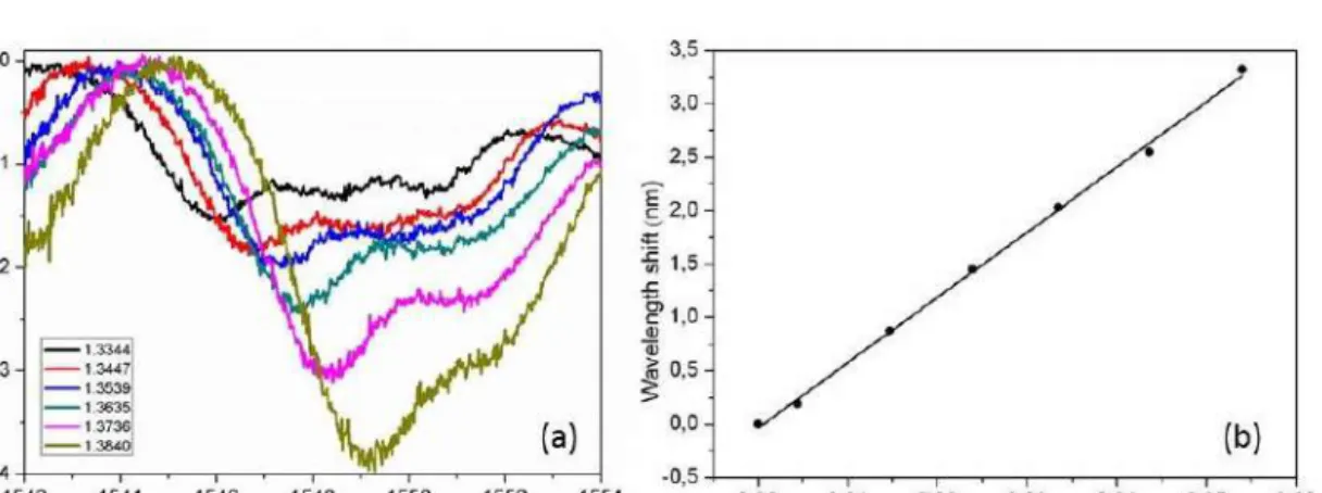
To characterize the sensitivity of our device, we filled it with different concentrations of D- glucose solution, whose refractive index values are already tabulated19. Figure 4(a) shows the results of this refractive index sensing with six different D-glucose solutions for the resonance at 1548 nm. A shift of the resonance peak position, as determined with a Lorentzian fitting is clearly visible towards higher wavelength when the refractive index of the solution increases.
Moreover, Fig. 4(b) shows that there is a linear shift of the resonance position with the refractive index change. Based on the data from Fig 4 (b) we can say that the sensitivity of our device is around 61 ± 1 nm/RIU, with a detection limit of (0.0048 ± 0.0003)RIU (calculated following the analysis in reference20). We expect an improvement in the detection limit of our system increasing the microresonator Q factor for example with a higher resonator diameter and developing new strategies to separate the resonator from the waveguide (for example using a critical point dryer21. We were able to perform refractive index measurements several times without damaging the sensor, intercalating them with water or ethanol cleaning steps.
Considering the free spectral range of the microresonator as the maximum resonance shift that we can unambiguously relate to a refractive index change, we can retrieve the dynamic range of our present device as 15 dB.
The demonstration of label-free biosensing with our chip exploited the high-affinity of the biotin-streptavidin binding, where the resonator surface was covered with a layer of biotin and the presence of streptavidin protein was detected in samples flowing in the chip. The functionalization of the integrated SU8 microresonator surface is performed following the protocol reported in the Experimental section. To check the affinity of the integrated resonator surface toward streptavidin, it was incubated with Cy5- conjugated fluorescent streptavidin solution. In the inset of Fig. 5(a) the fluorescence image of the resonator is shown, demonstrating that with the developed protocol the resonator surface is homogeneously functionalized with biotin.
Figure 4. (a) Resonance at ~1544 nm (in air) for six different D-glucose solutions; the legend shows their refractive indices. (b) Representation and linear fitting of refractive index change versus wavelength shift for the six peaks in (a) with respect to pure water (see Supplementary material for fitting equation details); error bars, calculated from the accuracy in the Lorentzian fitting of the resonance dips, are smaller than symbols.
Figure 3. (a) Scanning electron microscope image of the free-standing microring resonator and the coupling waveguide fabricated by two photon polymerization (external ring diameter 50 µm); (b) Transmission spectra of the microring resonator in air.
Lab on a Chip Accepted Manuscript
Published on 24 April 2019. Downloaded by KEAN UNIVERSITY on 4/25/2019 2:25:18 PM.
View Article Online DOI: 10.1039/C9LC00174C
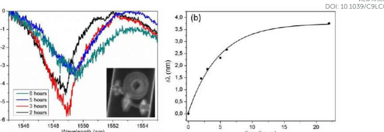
A second chip that followed the same functionalization protocol, but without the fluorescent streptavidin incubation step, was used to perform the detection of streptavidin bonding to the functionalized surface using the change in the refractive index of the resonator surface. First, the chip was filled with PBS and afterwards a 500 nM streptavidin solution in PBS was injected and incubated for 22 h.
Measurements of the sensor spectrum were taken at the following time points: 2, 3, 5, 6 and 22 hours. After each spectrum acquisition, the streptavidin solution was made to flow for 1 minute in order to refresh the solution in contact with the resonator. The spectra acquired at the different time points are then compared to the initial one, corresponding to pure PBS solution, and the wavelength shift of one resonance peak is retrieved. Figure 5(a) reports the transmission spectra for the first four measurements, where the shift of resonance at ~1550nm is visible. The full analysis of the experiment is shown in Fig. 5(b), which depicts the variation of the resonance wavelength (retrieved from a Lorentzian fit) as a function of time. We can observe an exponential saturation trend on the resonance shift with time (see Supplementary materials for details), which evidences that we are reaching the maximum number of molecules that might be attached to the sensor surface.
The surface density of streptavidin molecules bound to the surface (σp) can be estimated using the equation20:
(2)
𝛿𝜆
𝜆= 𝜎𝑝𝛼𝑒𝑥
2𝜋 𝑛2𝑚― 𝑛2𝑠 𝜀0𝜆2
𝑛𝑚 𝑛2𝑠 𝑆
Where αex is the excess polarizability of the streptavidin molecule (4πε0∙(3.2 x 10⁻²¹) cm3, from reference22,23), nm is the SU8 refractive index (1.57), ns is the PBS refractive index (1.35), S is the refractive index sensitivity of our sensor calculated previously (61 nm/RIU), λ is the resonance wavelength (1550 nm) and δλ is the resonance shift for each specific measurement. With these values, and taking into account the detection limit of our resonator (that gives a minimum detectable resonance shift of 0.29 ± 0.02 nm), the minimum surface density increase that we will be able to detect is (67 ± 5) x 103 molecules/µm2. It should be noted that the connection between this surface concentration and that originally present in the sample
volume depends on the efficacy of the sample-sensor interaction, which in turn is related to the binding affinity, the fluidic geometry and the measurement protocol. These aspects will be optimized in future work. On the other hand, the maximum number of molecules that our sensor supports (taking into account the exponential trend of the resonance shift) can be estimated as (820 ± 31) x 103 molecules /µm2. This value is less than expected, indicating that the biotin monolayer is not completely covering the microresonator surface.
This results in a dynamic range of 11 dB that we expect to increase by improving the coating process.
Conclusions
In this work we are presenting a label-free optofluidic sensor fabricated by hybrid femtosecond laser micromachining. It consists of a glass microfluidic chip, fabricated by FLICE, which contains a WGM microresonator fabricated by 2PP from SU8 photoresist. After the fluidic and optical assembly, we obtain a robust, portable and easy to use LOC device. It presents a rather good refractive index sensitivity of 61 nm/RIU that is mainly limited by the overcoupling between the coupling waveguide and microresonator, which we expect to improve using novel development protocols. The biosensing capabilities of the device have been demonstrated exploiting the biotin- streptavidin binding affinity, obtaining a minimum measurable surface density increase of 67 x 103 molecules /µm2. Despite its moderate sensitivity, our system is completely monolithic, providing clear advantages in terms of robustness, handling and reproducibility, which are fundamental characteristic for real- world biosensing applications.
Author Contributions.
Conceptualization: R.M.V, L.K, P.O. and R.O., Data Curation: E.L.
and R.M.V., Formal Analysis: R.M.V., E.L. and L.K., Funding Acquisition: R.M.V., L.K., P.O. and R. O., Investigation: R.M.V., L.K., E.L. and B.H., Project Administration: R.M.V. and R.O., Validation: R.M.V., E.L. and L.K., Visualization: R.M.V., Writing-
Figure 5. (a) Resonance at 1549 nm for 4 different streptavidin incubation times. Inset; fluorescent image of the Biotin-functionalized microresonator incubated in fluorescent streptavidin. (b) Wavelength shift versus incubation time and exponential fitting; error bars, calculated from the accuracy in the Lorentzian fitting of the resonance dips, are smaller than symbols.
Lab on a Chip Accepted Manuscript
Published on 24 April 2019. Downloaded by KEAN UNIVERSITY on 4/25/2019 2:25:18 PM.
View Article Online DOI: 10.1039/C9LC00174C
ARTICLE Lab on a Chip
6 | J. Name., 2012, 00, 1-6 This journal is © The Royal Society of Chemistry 20xx original draft: R.M.V., L.K., P.O. and R.O., Writing-review and
editing: R.M.V. and R.O.
Conflicts of interest.
There are no conflicts to declare.Acknowledgements
This work was supported by funding received from the CONCERT-Japan Photonic Manufacturing Joint Call (FEASIBLE project). This work was supported by the GINOP-2.3.2-15-2016- 00001 and the GINOP-2.3.3-15-2016-00040 programs. This project also received funding from the European Union’s Horizon 2020 research and innovation programme under grant agreement No. 654148 Laserlab-Europe.
References
1 M.S. Luchansky and R.C. Bailey, Anal. Chem., 2012, 84, 793.
2 J. Homola, Chem. Rev., 2008, 108, pp 462.
3 K.M Mayer and J.H. Hafner, Chem. Rev., 2011, 111, 3828.
4 K.E. Zinoviev, A. Belén González-Guerrero, C. Domínguez and L. M. Lechuga, J. Lightwave Technol., 2012, 29, 1926.
5 A. Crespi, Y. Gu, B. Ngamsom, H. J. W. M. Hoekstra, C. Dongre, M. Pollnau, R. Ramponi, H.H. van den Vlekkert, P. Watts, G.
Cerullo and R. Osellame, Lab Chip, 2010,10, 1167.
6 A. Mathesz, S. Valkai, A. Újvárosy, B. Aekbote, O. Sipos, B.
Stercz, B. Kocsis, D. Szabó and A. Dér, Optofluidics, Microfluidics and Nanofluidics, 2015, 2, 15.
7 M.G. Scullion, A. Di Falco and T.F. Krauss, Biosensors and Bioelectronics, 2011, 27, 101.
8 F. Vollmer and S. Arnold, Nature Methods, 2008, 5, 591.
9 D.K. Armani, T.J. Kippenberg, S.M. Spillane and K.J. Vahala, Nature, 2003, 421, 925.
10 J. Song, J. Lin, J. Tang, Y. Liao, F. He, Z. Wang, L. Qiao, K.
Sugioka and Y. Cheng, Opt. Express, 2014, 22, 14792.
11 K. Dongwan, P. Popescu, M. Harfouche, J. Sendowski, M.E.
Dimotsantou, R. C. Flagan and A. Yariv, Opt. Lett., 2015, 40, 4106.
12 F. Sima, K. Sugioka, R. Martínez Vázquez, R. Osellame, L.
Kelemen and P. Ormos, Nanophotonics, 2018, 7, 613-634.
13 K. Sugioka, J. Xu, D. Wu, Y. Hanada, Z. Wang, Y. Cheng, and K.
Midorikawa, Lab Chip, 2014, 14, 3447.
14 L. Amato, Y. Gu, N. Bellini, S.M. Eaton, G. Cerullo, and R.
Osellame, Lab Chip, 2012, 12, 1135.
15 R. Osellame, H.J.W.M. Hoekstra, G. Cerullo, and M. Pollnau, Laser Photonics Rev., 2011, 5, 442.
16 T. Yang, P. Paiè, G. Nava, F. Bragheri, R. Martínez Vázquez, P.
Minzioni, M. Veglione, M. Di Tano, C. Mondello, R. Osellame, and I. Cristiani, Lab Chip, 2015, 15, 1262.
17 C. Y. Chao and L. J. Guo, Journal of Lightwave Technology, 2006, 24, 1395.
18 J. Wu, X. Guo, A. P. Zhang and H.-Y. Tam, Opt. Express, 2015, 23, 29708.
19 David R. Lide, Handbook of Chemistry and Physics, CRC Press, 2003-2004.
20 I.M. White and X. Fan, Opt. Express, 2008, 16, 1020.
21 K. Obata, A. El-Tamer, K. Ayman, A. Lothar, U. Hinze, Ulf, B.
Chichkov, Light: Science &Amp; Applications, 2013, 2, e116.
22 S. Arnold, M. Khoshsima, I. Teraoka, S. Holler and F. Vollmer, Opt. Lett., 2003, 28, 272.
23 M.G. Scullion, A. Di Falco and T.F. Krauss, Biosensors and Bioelectronics, 2011, 27, 101.
Lab on a Chip Accepted Manuscript
Published on 24 April 2019. Downloaded by KEAN UNIVERSITY on 4/25/2019 2:25:18 PM.
View Article Online DOI: 10.1039/C9LC00174C
Hybrid Femtosecond laser fabrication of a glass lab-on-chip, with an integrated whispering gallery mode resonator, for label free biomolecule sensing.
Lab on a Chip Accepted Manuscript
Published on 24 April 2019. Downloaded by KEAN UNIVERSITY on 4/25/2019 2:25:18 PM.