AIP Conference Proceedings 2186, 040002 (2019); https://doi.org/10.1063/1.5137931 2186, 040002
© 2019 Author(s).
Swift heavy ion irradiated planar waveguides in a rare earth doped tungsten Tellurite glass and a tungstate crystal
Cite as: AIP Conference Proceedings 2186, 040002 (2019); https://doi.org/10.1063/1.5137931 Published Online: 10 December 2019
I. Bányász, G. U. L. Nagy, I. Rajta, V. Havránek, V. Vosecek, M. Fried, P. Petrik, E. Agócs, B. Kalas, M. Veres, and R. Holomb
Swift Heavy Ion Irradiated Planar Waveguides in a Rare Earth Doped Tungsten Tellurite Glass and a Tungstate
Crystal
I. Bányász
1, a), G.U.L. Nagy
2, I. Rajta
2, V. Havránek
3, V. Vosecek
3, M. Fried
4, P.
Petrik
4, E. Agócs
4,B. Kalas
4,M. Veres
1and R. Holomb
11 Wigner Research Centre for Physics, Hungarian Academy of Sciences, P.O.B. 49, H-1525, Budapest, Hungary
2 MTA Atomki, Institute for Nuclear Research, Hungarian Academy of Sciences, H-4001 Debrecen, P.O. Box 51 Hungary
3 Nuclear Physics Institute AV CR, Řež near Prague, 250 68, Czech Republic
4. Research Institute for Technical Physics and Materials Science, Centre for Energy Research, Hungarian Academy of Sciences, Budapest, P.O.B. 49, H-1525 Hungary
a) Corresponding author: banyasz.istvan@wigner.mta.hu
Abstract. Planar optical waveguides were designed and fabricated in an Er-doped Tungsten- Tellurite oxide glass and in a KDy (WO4)2 crystal by swift heavy ion irradiation. 12.5 MeV Au5+ ions were used in the first case and 10.5 MeV N4+
ions in the second one. Irradiated fluences were very low: 7·1014 ions/cm2 in the first experiment, and 4·1015 ions/cm2 ions/cm2 in the second one. Micro Raman studies of both waveguides showed structural changes in the irradiated samples. Ellipsometric measurements showed the existence of ion beam irradiated thin film structures in both samples.
M-line spectroscopic measurements were carried out to check functionality of the ion beam irradiated planar optical waveguides. One guided mode was detected in both samples at the wavelength of 632.8 nm both in TE and TM modes.
However, amplitude and width of the detected m-lines indicate high propagation losses. According to our previous experiences, stepwise thermal annealing can largely reduce propagation losses, and even allow for guiding at the 1550 nm telecom band.
INTRODUCTION
Ion beam techniques are among the best methods for optical waveguide fabrication in crystalline and amorphous materials. The first report on waveguide fabrication in fused silica using proton beam was published by Schineller et al. in 1968 [1]. An important monograph of this field was written by Townsend et al. [2]. A detailed review of ion- implanted waveguides in optical materials has recently been published by Chen et al. [3].
Formation of adequate refractive index changes for waveguide fabrication requires relatively high fluences, in the 1015 - 1017 ions/cm2 range, especially when mass and energy of the implanted ion are low. When ion mass and energy are higher, the electronic interaction becomes predominant over the nuclear one. First studies on the effects of swift heavy ion irradiation on the optical properties of materials date back to the 1990’s [4]. Fabrication of waveguides with swift heavy and medium-light ions was demonstrated especially in LiNbO3 crystals. The refractive index change needed to fabricate an optical waveguide has been produced either by the electronic interaction between the ions and the target atoms or by the creation of an optical barrier at the stopping range of the ions [5-7].
DESIGN AND FABRICATION OF THE WAVEGUIDES
The irradiations were carried out at Tandetron Laboratory of the Nuclear Physics Institute AV CR, Řež, Czech Republic. Ion species, energies and fluences for the fabrication of the planar optical waveguides were chosen so that the irradiated samples could work well at the design wavelengths.
The two materials were chosen because of their high importance in modern integrated optics. Rare earth doped glasses are widely used as lasers and amplifiers. However, due to their high susceptibility to chemical processing, alternative fabrication methods, such as direct laser writing and ion beam implantation were developed [8, 9]. Gold was chosen as the implanted ion to provide plasmonic enhancement of the luminescence of the Er-doped Tungsten Tellurite glass, and at the same time create a planar waveguide. Electronic and nuclear energy losses as well as Au ion ranges were calculated using the SRIM code [10], and are presented in Figure 1.a) and b).
FIGURE 1. a) Electronic and nuclear energy loss vs. depth of 12.5 MeV Au5+ ions in Er-doped Te – W glass. b). Distribution of the implanted Au atoms in Er-doped Te – W glass.
It can be seen in Figure 1. that electronic and nuclear energy losses are of the same order of magnitude. The implanted gold atoms form a thick layer of 1.5 μm (at the level 1/e in Figure 1. b), centered at 2.1 μm.
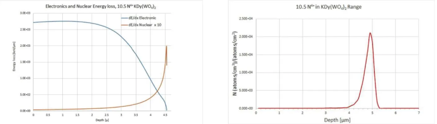
KDy (WO4)2, as well as other tungstate crystals, is also a widely used material for the fabrication of integrated optical amplifiers and lasers [11-13]. Electronic and nuclear energy losses as well as N ion ranges were calculated using the SRIM code are shown in Figure 2.a) and b).
FIGURE 2. a) Electronic and nuclear energy loss vs. depth of 10.5 MeV N4+ ions in the KDy (WO4)2 crystal. b). Distribution of the implanted N atoms in the KDy (WO4)2 crystal.
Irradiated fluences were very low: 7·1014 ions/cm2 in the first experiment, and 4·1015 ions/cm2 in the second one.
MICRO RAMAN MEASUREMENTS
The irradiated samples were studied by micro Raman spectroscopy to reveal structural changes due to the ion irradiation. The results are presented in Figure 3.a) and b).
FIGURE 3. a) Micro Raman spectra of the bulk and 12.5 MeV Au5+ irradiated Er-doped Te-W-glass. b) Micro Raman spectra of the 10.5 MeV N4+ irradiated KDy (WO4)2 crystal.
Irradiation by the gold ions caused the appearance of a new band in the Raman spectrum of the Er-doped Te-W- glass, centered at 119.2 cm-1. Similarly, a new band was created at 950 cm-1 in the Raman spectrum of the 10.5 MeV N4+ irradiated KDy (WO4)2 crystal.
SPECTROSCOPIC ELLIPSOMETRIC MEASUREMENTS
Both waveguides were measured by a
WOOLLAM M-2000DI spectroscopic ellipsometer (SE) (λ = 193- 1690 nm). A three-layer optical model was applied in the evaluation of the spectroscopic ellipsometry (SE) data. Results are shown in Figure 4.
FIGURE 4. Depth profiles of the optical constants at 633 nm calculated from SE measurements a) of the 12.5 MeV Au5+
irradiated Er-doped Te-W-glass. b) of the 10.5 MeV N4+ irradiated KDy (WO4)2 crystal.
M-LINE SPECTROSCOPY
Functionality of the planar waveguides was tested by m-line spectroscopy. A Metricon 2010M Prism Coupler was used at 632.8 nm and 1534.9 nm, both in TE and TM modes. Guiding in the as-implanted waveguides could be proved only at the wavelength of 632.8 nm. TM m-line spectra taken at 632.8 nm are presented in Figure 5.
Effective refractive indices of the detected modes can be seen in Table 1.
TABLE 1. Effective refractive indices of the detected modes at 632.8 nm.
Waveguide name neff TE neff TM
Er-doped Te-W glass 2.1596 1.9564
KDy(WO4)2 crystal - 2.0665
FIGURE 5. M-line spectra at 633 nm in TM mode a) of the 12.5 MeV Au5+ irradiated Er-doped Te-W-glass. b) of the 10.5 MeV N4+ irradiated KDy (WO4)2 crystal.
CONCLUSION
Fabrication of planar optical waveguides via swift heavy ion irradiation at low fluences in an Er-doped Tungsten – Tellurite glass and KDy (WO4)2 crystal was devised and performed. Structural studies proved the creation of the thin layers. M-line spectroscopic measurements of the samples showed that both waveguides could support one guided mode at 632.8 nm. However, the low amplitudes of the detected modes indicate relatively high propagation losses. Both the relevant scientific literature and our own experiences suggest that stepwise annealing of both samples could significantly reduce propagation losses of the waveguides. Even guiding at the telecom band of 1.5 μm can be expected.
REFERENCES
1. E. R. Schineller, R. P. Flam, and D. W. Wilmot, J. Opt. Soc. Am. 58, 1171, (1968)
2. P. D. Townsend, P. J. Chandler and L . Zhang Optical Effects of Ion Implantation, Chapters 5– 7, (Cambridge University Press Cambridge, U.K., (1994)
3. F. Chen, X. L.Wang and K.M. Wang, Opt. Mat., 29, 1523-1542, (2007).
4. P. Sreeramana Aithal, H.S. Nagaraja, P. Mohan Rao, D.K. Avasthi, Asati Sarma, Journal of Applied Physics, 81 7526 (1997)
5. G. Szenes, Phys. Rev. B 52 6154-6157 (1995).
6. G.G. Bentini, M. Bianconi, L. Correa, M. Chiarini, P. Mazzoldi, C. Sada, N. Argiolas, M. Bazzan, R. Guzzi, Journal of Applied Physics, 96 242-247 (2004)
7. J. Olivares, G. García, A. García-Navarro, F. Agulló-López, O. Caballero, A. García-Cabañes, Appl. Phys.
Lett., 86 183501 (2005)
8. S. Berneschi, G. Nunzi Conti, I. Bányász, A. Watterich, N.Q. Khanh, M. Fried, F. Pászti, M. Brenci, S. Pelli, G.C. Righini, Appl. Phys. Lett 90 121136 (2007
9. I. Bányász, S. Berneschi, M. Bettinelli, M. Brenci, M. Fried, N.Q. Khanh, T. Lohner, G. Nunzi Conti, S. Pelli, P. Petrik, G.C. Righini, A. Speghini, A. Watterich, Z. Zolnai, IEEE Photonics J. 4 721-727, (2012).
10. J.F. Ziegler, J.P. Biersack, Nuclear Instruments and Methods in Physics Research Section B, 268 1818-1823 (2010)
11. S.V. Kurbasov, L.L. Losev, Optics Communications 168 227–232 (1999)
12. J.Liu, J. M. Cano Torres, F. Esteban-Betego, et al. , Optics & Laser Technology 39 558–561 (2007)
13. C. A. Merchant, P. Scrutton, S. García-Blanco, C. Hnatovsky, R. S. Taylor, A. García-Navarro, G. García, F.
Agulló-López, J. Olivares, A. S. Helmy and J. S. Aitchison, IEEE J. Quantum Electronics 45 373-379 (2009)