Írta: Sima Dezső, Szénási Sándor, Tóth Ákos
MASSZÍVAN
PÁRHUZAMOS
PROGRAMOZÁS GPGPU-K ALKALMAZÁSÁVAL
PÁRHUZAMOS SZÁMÍTÁSTECHNIKA MODUL
PROAKTÍV INFORMATIKAI MODULFEJLESZTÉS
Lektorálta: oktatói munkaközösség
COPYRIGHT:
2011-2016, Dr. Sima Dezső, Szénási Sándor, Tóth Ákos, Óbudai Egyetem, Neumann János Informatikai Kar
LEKTORÁLTA: oktatói munkaközösség
Creative Commons NonCommercial-NoDerivs 3.0 (CC BY-NC-ND 3.0)
A szerző nevének feltüntetése mellett nem kereskedelmi céllal szabadon másolható, terjeszthető, megjelentethető és előadható, de nem módosítható.
TÁMOGATÁS:
Készült a TÁMOP-4.1.2-08/2/A/KMR-2009-0053 számú, „Proaktív informatikai modulfejlesztés (PRIM1): IT Szolgáltatásmenedzsment modul és Többszálas processzorok és programozásuk modul” című pályázat keretében
KÉSZÜLT: a Typotex Kiadó gondozásában FELELŐS VEZETŐ: Votisky Zsuzsa
ISBN 978-963-279-560-7
KULCSSZAVAK:
GPGPU, grafikai kártya, architektúrák, CUDA, OpenCL, adatpárhuzamosság, programozás, optimalizáció
ÖSSZEFOGLALÓ:
A processzorarchitektúrák elmúlt években bekövetkezett fejlődésének egyik szignifikáns eredménye az általános célú grafikai kártyák (GPGPU-k) és az alkalmazásukhoz szükséges szoftverprogramozási környezetek megjelenése. A tárgy keretében a hallgatók először megismerkednek a GPGPU-k általános felépítésével, a legfontosabb reprezentáns architektúrákkal. Ezt követően gyakorlati ismereteket szereznek az adatpárhuzamos
programozási modellen keresztül történő feladatmegoldásban, a számításigényes feladatok futásának gyorsításában. A tárgy keretein belül megjelennek a napjainkban legelterjedtebb GPGPU programozási környezetek (Nvidia CUDA illetve OpenCL), amelyekkel kapcsolatban a hallgatók megismerik azok felépítését, használatát (eszközök kezelése,
memóriaműveletek, kernelek készítése, kernelek végrehajtása), majd pedig gyakorlati feladatok megoldásán keresztül (alapvető mátrixműveletek, minimum-maximum kiválasztás stb.) bővíthetik programozási ismereteiket. A programozási környezetek bemutatásán túlmenően hangsúlyozottan megjelenik az újszerű eszközök speciális lehetőségeinek szerepe az optimalizáció területén (megosztott memória használata, atomi műveletek stb.).
Contents
GPGPUs/DPAs
GPGPUs/DPAs 5.1. Case example 1: Nvidia’s Fermi family of cores
GPGPUs/DPAs 5.2. Case example 2: AMD’s Cayman core
GPGPUs/DPAs 6. Integrated CPUs/GPUs
GPGPUs/DPAs 7. References
GP GPU alapok
CUDA környezet alapjai
CUDA haladó ismeretek
OpenCL alapok
OpenCL programozás
OpenCL programozás 2.
OpenCL programozás 3.
Dezső Sima
GPGPUs/DPAs
2. Basics of the SIMT execution Contents
1.Introduction
3. Overview of GPGPUs
4. Overview of data parallel accelerators
1. Introduction
Vertex
Edge Surface
Vertices
• have three spatial coordinates
• supplementary information necessary to render the object, such as
• color
• texture
• reflectance properties
• etc.
Representation of objects by triangles
1. Introduction (1)
1. Introduction (2)
Example: Triangle representation of a dolphin [149]
Main types of shaders in GPUs
Shaders
Geometry shaders Vertex shaders Pixel shaders
(Fragment shaders) Transform each vertex’s
3D-position in the virtual space to the 2D coordinate,
at which it appears on the screen
Calculate the color of the pixels
Can add or remove vertices from a mesh
1. Introduction (3)
DirectX version Pixel SM Vertex SM Supporting OS 8.0 (11/2000) 1.0, 1.1 1.0, 1.1 Windows 2000
8.1 (10/2001) 1.2, 1.3, 1.4 1.0, 1.1 Windows XP/ Windows Server 2003
9.0 (12/2002) 2.0 2.0 9.0a (3/2003) 2_A, 2_B 2.x
9.0c (8/2004) 3.0 3.0 Windows XP SP2 10.0 (11/2006) 4.0 4.0 Windows Vista
10.1 (2/2008) 4.1 4.1 Windows Vista SP1/
Windows Server 2008 11 (10/2009) 5.0 5.0 Windows7/
Windows Vista SP1/
Windows Server 2008 SP2 Table 1.1: Pixel/vertex shader models (SM) supported by subsequent versions of DirectX
and MS’s OSs [18], [21]
1. Introduction (4)
DirectX: Microsoft’s API set for MM/3D
Convergence of important features of the vertex and pixel shader models Subsequent shader models introduce typically, a number of new/enhanced features.
Shader model 2 [19]
• Different precision requirements
• Vertex shader: FP32 (coordinates)
• Pixel shader: FX24 (3 colors x 8)
• Different instructions
• Different resources (e.g. registers)
Differences between the vertex and pixel shader models in subsequent shader models concerning precision requirements, instruction sets and programming resources.
Shader model 3 [19]
• Unified precision requirements for both shaders (FP32)
with the option to specify partial precision (FP16 or FP24) by adding a modifier to the shader code
• Different instructions
• Different resources (e.g. registers)
1. Introduction (5)
Different data types
Shader model 4 (introduced with DirectX10) [20]
• Unified precision requirements for both shaders (FP32) with the possibility to use new data formats.
• Unified instruction set
• Unified resources (e.g. temporary and constant registers) Shader architectures of GPUs prior to SM4
GPUs prior to SM4 (DirectX 10):
have separate vertex and pixel units with different features.
Drawback of having separate units for vertex and pixel shading
• Inefficiency of the hardware implementation
• (Vertex shaders and pixel shaders often have complementary load patterns [21]).
1. Introduction (6)
Unified shader model (introduced in the SM 4.0 of DirectX 10.0)
The same (programmable) processor can be used to implement all shaders;
• the vertex shader
• the pixel shader and
• the geometry shader (new feature of the SMl 4) Unified, programable shader architecture
1. Introduction (7)
Figure 1.1: Principle of the unified shader architecture [22]
1. Introduction (8)
Based on its FP32 computing capability and the large number of FP-units available
the unified shader is a prospective candidate for speeding up HPC!
GPUs with unified shader architectures also termed as GPGPUs
(General Purpose GPUs)
1. Introduction (9)
or cGPUs
(computational GPUs)
1. Introduction (10)
Peak FP32/FP64 performance of Nvidia’s GPUs vs Intel’ P4 and Core2 processors [43]
Peak FP32 performance of AMD’s GPGPUs [87]
1. Introduction (11)
1. Introduction (12)
Evolution of the FP-32 performance of GPGPUs [44]
Evolution of the bandwidth of Nvidia’s GPU’s vs Intel’s P4 and Core2 processors [43]
1. Introduction (13)
Figure 1.2: Contrasting the utilization of the silicon area in CPUs and GPUs [11]
1. Introduction (14)
• Less area for control since GPGPUs have simplified control (same instruction for all ALUs)
• Less area for caches since GPGPUs support massive multithereading to hide latency of long operations, such as memory accesses in case of cache misses.
2. Basics of the SIMT execution
Main alternatives of data parallel execution models
Data parallel execution models
SIMD execution SIMT execution
• One dimensional data parallel execution, i.e. it performs the same operation on all elements of given
FX/FP input vectors
• Two dimensional data parallel execution, i.e. it performs the same operation on all elements of a given
FX/FP input array (matrix)
E.g. 2. and 3. generation superscalars
GPGPUs,
data parallel accelerators
• data dependent flow control as well as
• barrier synchronization
• is massively multithreaded, and provides
Needs an FX/FP SIMD extension
of the ISA Assumes an entirely new specification, that is done at the virtual machine level
(pseudo ISA level)
2. Basics of the SIMT execution (1)
2. Basics of the SIMT execution (2)
Remarks
1) SIMT execution is also termed as SPMD (Single_Program Multiple_Data) execution (Nvidia).
2) The SIMT execution model is a low level execution model that needs to be complemented with further models, such as the model of computational resources or the memory model, not discussed here.
2. Basics of the SIMT execution (3)
Specification levels of GPGPUs GPGPUs are specified at two levels
• at a virtual machine level (pseudo ISA level, pseudo assembly level, intermediate level) and
• at the object code level (real GPGPU ISA level).
Object code level
Virtual machine level
HLL
HLL application
HLL compiler
Pseudo assembly code AMD IL
Nvidia AMD
CUDA
OpenCL (Brook+) OpenCL
nvcc nvopencc
PTX
(brcc)
2. Basics of the SIMT execution (4)
Virtual machine level (Compatible code)
The process of program development
HLL level
Becomes a two-phase process
• Phase 1: Compiling the HLL application to pseudo assembly code
The compiled pseudo ISA code (PTX code/IL code) remains independent from the
actual hardware implementation of a target GPGPU, i.e. it is portable over different GPGPU families.
Compiling a PTX/IL file to a GPGPU that misses features supported by the particular PTX/IL version however, may need emulation for features not implemented in hardware.
Pseudo assembly code
GPU specific binary code Pseudo assembly – GPU compiler
AMD IL
Target binary CAL compiler
Nvidia AMD
PTX
CUBIN file
2. Basics of the SIMT execution (5)
Virtual machine level (Compatible code)
CUDA driver The process of program development-2
Object code level (GPU bound)
• Phase 2: Compiling the pseudo assembly code to GPU specific binary code
The object code (GPGPU code, e.g. a CUBIN file) is forward portable, but forward portabilility is provided typically only within major GPGPU versions, such as Nvidia’s compute capability versions 1.x or 2.x.
• The compiled pseudo ISA code (PTX code/IL code) remains independent from the
actual hardware implementation of a target GPGPU, i.e. it is portable over subsequent GPGPU families.
Forward portability of the object code (GPGPU code, e.g. CUBIN code) is provided however, typically only within major versions.
• Compiling a PTX/IL file to a GPGPU that misses features supported by the particular PTX/IL version however, may need emulation for features not implemented in hardware.
This slows down execution.
• Portability of pseudo assembly code (Nvidia’s PTX code or AMD’s IL code) is highly
advantageous in the recent rapid evolution phase of GPGPU technology as it results in less costs for code refactoring.
Code refactoring costs are a kind of software maintenance costs that arise when the user switches from a given generation to a subsequent GPGPU generation (like from GT200 based devices to GF100 or GF110-based devices) or to a new software environment (like from CUDA 1.x SDK to CUDA 2.x or from CUDA 3.x SDK to CUDA 4.x SDK).
Benefits of the portability of the pseudo assembly code
2. Basics of the SIMT execution (6)
Remark
• For Java there is also an inherent pseudo ISA definition, called the Java bytecode.
• Applications written in Java will first be compiled to the platform independent Java bytecode.
• The Java bytecode will then either be interpreted by the Java Runtime Environment (JRE) installed on the end user’s computer or compiled at runtime by the Just-In-Time (JIT) compiler of the end user.
The virtual machine concept underlying both Nvidia’s and AMD’s GPGPUs is similar to the virtual machine concept underlying Java.
2. Basics of the SIMT execution (7)
At the virtual machine level GPGPU computing is specified by
• the SIMT computational model and
• the related pseudo iSA of the GPGPU.
Specification GPGPU computing at the virtual machine level
2. Basics of the SIMT execution (8)
The SIMT computational model
It covers the following three abstractions
Model of computational
resources
The memory model
Model of SIMT execution
Figure 2.2: Key abstractions of the SIMT computational model
2. Basics of the SIMT execution (9)
2. Basics of the SIMT execution (10)
1. The model of computational resources
It specifies the computational resources available at virtual machine level (the pseudo ISA level).
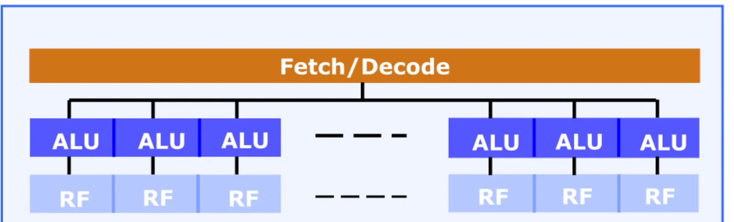
• Basic elements of the computational resources are SIMT cores.
Figure 2.3: Basic structure of the underlying SIMD cores ALUs operate in a pipelined fashion, to be discussed later.
First, let’s discuss the basic structure of the underlying SIMD cores.
SIMD cores execute the same instruction stream on a number of ALUs (e.g. on 32 ALUs), i.e. all ALUs perform typically the same operations in parallel.
• SIMT cores are specific SIMD cores, i.e. SIMD cores enhanced for efficient multithreading.
Efficient multithreading means zero-cycle penalty context switches, to be discussed later.
SIMD core ALU
Fetch/Decode
ALU ALU ALU ALU
SIMD ALUs operate according to the load/store principle, like RISC processors i.e.
The load/store principle of operation takes for granted the availability of a register file (RF) for each ALU.
RF
Figure 2.4: Principle of operation of a SIMD ALU
2. Basics of the SIMT execution (11)
• they load operands from the memory,
• perform operations in the “register space” i.e.
• they take operands from the register file,
• perform the prescribed operations and
• store operation results again into the register file, and
• store (write back) final results into the memory.
Load/Store Memory
ALU
As a consequence of the chosen principle of execution each ALU is allocated a register file (RF) that is a number of working registers.
Figure 2.5: Main functional blocks of a SIMD core
2. Basics of the SIMT execution (12)
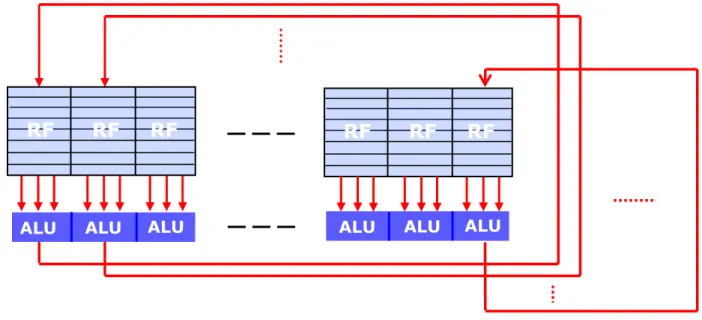
Fetch/Decode
ALU ALU ALU
RF RF RF
ALU ALU ALU RF RF
RF
Remark
Figure 2.6: Allocation of distinct parts of a large register file to the private register sets of the ALUs The register sets (RF) allocated to each ALU are actually, parts of a large enough register file.
2. Basics of the SIMT execution (13)
ALU ALU
ALU ALU ALU
RF RF RF RF RF RF
ALU ALU ALU
Basic operations of the underlying SIMD ALUs
• and are pipelined, i.e.
• They execute basically FP32 Multiply-Add instructions of the form a x b + c ,
• need a few number of clock cycles, e.g. 2 or 4 shader cycles
to present the results of the FP32 Multiply-Add operations to the RF, Without further enhancements
the peak performance of the ALUs is 2 FP32 operations/cycle.
2. Basics of the SIMT execution (14)
• capable of starting a new operation every new clock cycle, (more precisely, every new shader clock cycle), and
ALU RF
• FX32 operations,
• FP64 operations,
• FX/FP conversions,
• single precision trigonometric functions (to calculate reflections, shading etc.).
2. Basics of the SIMT execution (15)
Beyond the basic operations the SIMD cores provide a set of further computational capabilities, such as
Note
Computational capabilities specified at the pseudo ISA level (intermediate level) are
• by firmware (i.e. microcoded,
• or even by emulation during the second phase of compilation.
• typically implemented in hardware.
Nevertheless, it is also possible to implement some compute capabilities
Aim of multithreading in GPGPUs
Speeding up computations by eliminating thread stalls due to long latency operations.
Achieved by suspending stalled threads from execution and allocating free computational resources to runable threads.
2. Basics of the SIMT execution (16)
Enhancing SIMD cores to SIMT cores
This allows to lay less emphasis on the implementation of sophisticated cache systems and utilize redeemed silicon area (used otherwise for implementing caches)
for performing computations.
SIMT cores are enhanced SIMD cores that provide an effective support of multithreading
Effective implementation of multithreading
requires that thread switches, called context switches, do not cause cycle penalties.
• providing and maintaining separate contexts for each thread, and
• implementing a zero-cycle context switch mechanism.
Achieved by
2. Basics of the SIMT execution (17)
Figure 2.7: SIMT cores are specific SIMD cores providing separate thread contexts for each thread
2. Basics of the SIMT execution (18)
SIMT cores
= SIMD cores with per thread register files (designated as CTX in the figure)
ALU
Actual context Register file (RF)
Context switch
Fetch/Decode
SIMT core
ALU ALU
ALU ALU ALU ALU
CTX CTX
CTX CTX CTX CTX
CTX CTX
CTX CTX CTX CTX
CTX CTX
CTX CTX CTX CTX
CTX CTX
CTX CTX CTX CTX
CTX CTX
CTX CTX CTX CTX
CTX CTX
CTX CTX CTX CTX
2. Basics of the SIMT execution (19)
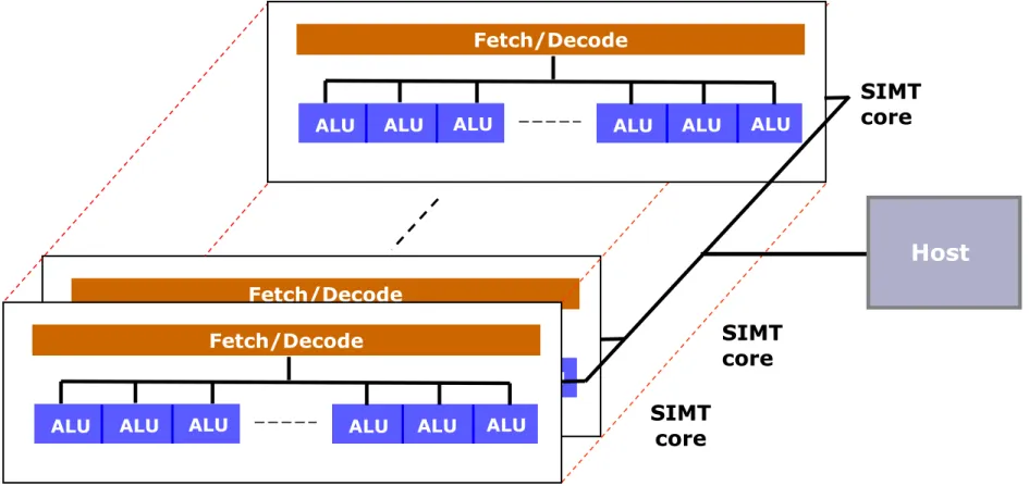
The GPGPU is assumed to have a number of SIMT cores and is connected to the host.
The final model of computational resources of GPGPUs at the virtual machine level
During SIMT execution 2-dimensional matrices will be mapped to the available SIMT cores.
Fetch/Decode
ALU ALU ALU ALU ALU ALU ALU ALU
SIMT core
SIMT core SIMT
core Fetch/Decode
ALU ALU ALU ALU ALU ALU ALU ALU
Fetch/Decode
ALU ALU ALU ALU ALU
ALU ALU ALU
Figure 2.8: The model of computational resources of GPGPUs
Host
SIMT core
Card ALU
Figure 2.9: The Platform model of OpenCL [144]
Remarks
1) The final model of computational resources of GPGPUs at the virtual machine level is similar to the platform model of OpenCL, given below assuming multiple cards.
2. Basics of the SIMT execution (20)
Figure 2.10: Simplified block diagram of the Cayman core (that underlies the HD 69xx series) [99]
2) Real GPGPU microarchitectures reflect the model of computational resources discussed at the virtual machine level.
2. Basics of the SIMT execution (21)
• streaming multiprocessor (Nvidia),
• superscalar shader processor (AMD),
• wide SIMD processor, CPU core (Intel).
3) Different manufacturers designate SIMT cores differently, such as
2. Basics of the SIMT execution (22)
Available data spaces
Register space Memory space
Local memory Constant memory Global memory Per thread
register file
The memory model
The memory model at the virtual machine level declares all data spaces available at this level along with their features, like their accessibility, access mode (read or write) access width etc.
Key components of available data spaces at the virtual machine level
(Local Data Share) (Constant Buffer) (Device memory)
Figure 2.11: Overview of available data spaces in GPGPUs
2. Basics of the SIMT execution (23)
Per thread register files
• Provide the working registers for the ALUs.
• There are private, per thread data spaces available for the execution of threads that is a prerequisite of zero-cycle context switches.
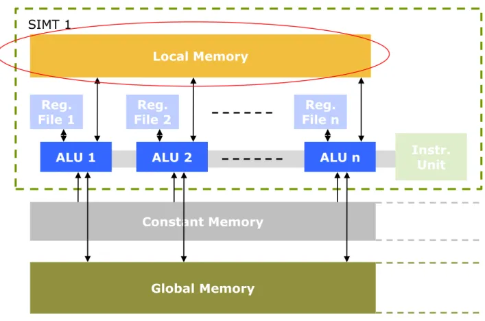
Local Memory
Reg.
File 1 Reg.
File 2 Reg.
File n
ALU 1 ALU 2 ALU n Instr.
Unit
Constant Memory
Global Memory SIMT 1
2. Basics of the SIMT execution (24)
Local memory
• On-die R/W data space that is accessible from all ALUs of a particular SIMT core.
• It allows sharing of data for the threads that are executing on the same SIMT core.
Local Memory
Reg.
File 1 Reg.
File 2 Reg.
File n
ALU 1 ALU 2 ALU n Instr.
Unit
Constant Memory
Global Memory SIMT 1
Figure 2.13: Key components of available data spaces at the level of SIMT cores
2. Basics of the SIMT execution (25)
Constant Memory
• On-die Read only data space that is accessible from all SIMT cores.
• It can be written by the system memory and is used to provide constants for all threads that are valid for the duration of a kernel execution with low access latency.
Local Memory ALU 1
Constant Memory
Global Memory SIMT 1
Reg.
File n ALU n Reg.
File 1
Local Memory ALU 1
SIMT m
Reg.
File n ALU n Reg.
File 1 GPGPU
2. Basics of the SIMT execution (26)
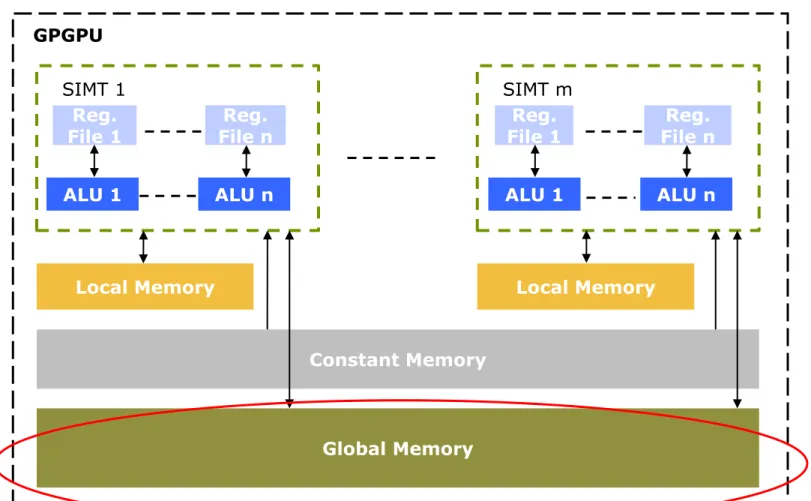
Global Memory
• Off-die R/W data space that is accessible for all SIMT cores of a GPGPU.
• It can be accessed by the system memory and is used to hold all instructions and data needed for executing kernels.
Local Memory ALU 1
Constant Memory
Global Memory SIMT 1
Reg.
File n ALU n Reg.
File 1
Local Memory ALU 1
SIMT m
Reg.
File n ALU n Reg.
File 1 GPGPU
Figure 2.15: Key components of available data spaces at the level of the GPGPU
2. Basics of the SIMT execution (27)
Remarks
1. AMD introduced Local memories, designated as Local Data Share, only along with their RV770-based HD 4xxx line in 2008.
2. Beyond the key data space elements available at the virtual machine level, discussed so far, there may be also other kinds of memories declared at the virtual machine level,
such as AMD’s Global Data Share, an on-chip Global memory introduced with their RV770-bssed HD 4xxx line in 2008).
3. Traditional caches are not visible at the virtual machine level, as they are transparent for program execution.
Nevertheless, more advanced GPGPUs allow an explicit cache management at the virtual machine level, by providing e.g. data prefetching.
In these cases the memory model needs to be extended with these caches accordingly.
4. Max. sizes of particular data spaces are specified by the related instruction formats of the intermediate language.
5. Actual sizes of particular data spaces are implementation dependent.
6. Nvidia and AMD designates different kinds of their data spaces differently, as shown below.
2. Basics of the SIMT execution (28)
Nvidia AMD
Register file Local Memory Constant Memory Global memory
Registers Shared Memory Constant Memory
Global Memory
General Purpose Registers Local Data Share Constant Register
Device memory
A set of SIMT cores with on-chip shared memory
A set of ALUs within the SIMT cores
Example 1: The platform model of PTX vers. 2.3 [147]
Nvidia
2. Basics of the SIMT execution (29)
Data space Access type Available Remark
General Purpose Registers R/W Per ALU Deafult: (127-2)*4
2*4 registers are reserved as Clause Temporary Registers
Local Data Share (LDS) R/W Per SIMD core On-chip memory that enables sharing of data between threads executing on a
particular SIMT
Constant Register (CR) R Per GPGPU 128 x 128 bit
Written by the host
Global Data Share R/W Per GPGPU On-chip memory that enables
sharing of data between threads executing on a GPGPU
Device Memory R/W GPGPU Read or written by the host
• Max. sizes of data spaces are specified along with the instructions formats of the intermediate language.
• The actual sizes of the data spaces are implementation dependent.
Table 2.1: Available data spaces in AMD’s IL vers. 2.0 [107]
Example 2: Data spaces in AMD’s IL vers. 2.0 (simplified)
Remarks
2. Basics of the SIMT execution (30)
Example: Simplified block diagram of the Cayman core (that underlies the HD 69xx series) [99]
2. Basics of the SIMT execution (31)
Multi-dimensional domain of
execution
Massive multithreading
The kernel concept
Concept of assigning work
to execution pipelines
Data dependent flow control
Barrier synchronization SIMT execution model
2. Basics of the SIMT execution (32)
The SIMT execution model
Key components of the SIMT execution model
The model of data sharing
Communication between
threads
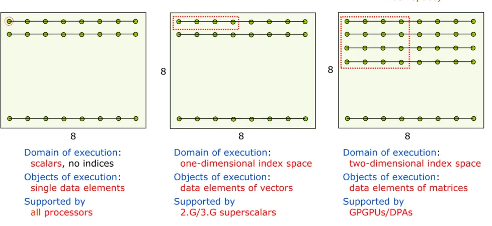
Scalar execution SIMD execution SIMT execution
(assuming a 2-dimensional index space)
Domain of execution:
scalars, no indices Objects of execution:
single data elements Supported by
all processors
Domain of execution:
one-dimensional index space Objects of execution:
data elements of vectors Supported by
2.G/3.G superscalars
Domain of execution:
two-dimensional index space Objects of execution:
data elements of matrices Supported by
GPGPUs/DPAs
Figure 2.16: Domains of execution in case of scalar, SIMD and SIMT execution
2. Basics of the SIMT execution (33)
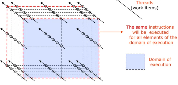
1. Multi-dimensional domain of execution
8
8
8 8
8 8
Domain of execution: index space of the execution
Figure 2.17: Parallel executable threads created and executed for each element of an execution domain
The same instructions will be executed for all elements of the domain of execution
2. Basics of the SIMT execution (34)
Threads (work items)
2. Massive multithreading
The programmer creates for each element of the index space, called the execution domain parallel executable threads that will be executed by the GPGPU or DPA.
Domain of execution
Figure 2.18: Interpretation of the kernel concept
The same instructions will be executed for all elements of the domain of execution
2. Basics of the SIMT execution (35)
Threads (work items)
3. The kernel concept-1
The programmer describes the set of operations to be done over the entire domain of execution by kernels.
Domain of execution Operations to be done
over the entire domain of execution
are described by a kernel
Kernels are specified at the HLL level and compiled to the intermediate level.
The kernel concept-2
Dedicated HLLs like OpenCL or CUDA C allow the programmer to define kernels, that, when called are executed n-times in parallel by n different threads,
as opposed to only once like regular C functions.
• Each thread that executes the kernel is given a unique identifier (thread ID, Work item ID) that is accessible within the kernel.
• using a declaration specifier (like _kernel in OpenCL or _global_ in CUDA C) and
• declaring the instructions to be executed.
• A kernel is defined by Specification of kernels
2. Basics of the SIMT execution (36)
The subsequent sample codes illustrate two kernels that adds two vectors (a/A) and (b/B) and store the result into vector (c/C).
CUDA C [43] OpenCL [144]
Sample codes for kernels
During execution each thread is identified by a unique identifier that is Remark
• int I in case of CUDA C, accessible through the threadIdx variable, and
• int id in case of OpenCL accessible through the built-in get_global_id() function.
2. Basics of the SIMT execution (37)
The kernel is invoked in CUDA C and OpenCL differently
• In CUDA C
by specifying the name of the kernel and the domain of execution [43]
• In OpenCL
by specifying the name of the kernel and the related configuration arguments, not detailed here [144].
Invocation of kernels
2. Basics of the SIMT execution (38)
4. Concept of assigning work to execution pipelines of the GPGPU
Typically a four step process
a) Segmenting the domain of execution to work allocation units b) Assigning work allocation units to SIMT cores for execution
c) Segmenting work allocation units into work scheduling units to be executed on the execution pipelines of the SIMT cores
d) Scheduling work scheduling units for execution to the execution pipelines of the SIMT cores
2. Basics of the SIMT execution (39)
4.a Segmenting the domain of execution to work allocation units-1
• The domain of execution will be broken down into equal sized ranges, called
work allocation units (WAUs), i.e. units of work that will be allocated to the SIMT cores as an entity.
2. Basics of the SIMT execution (40)
Global size m
Global size n
Domain of execution
Global size m
Global size n
Domain of execution
WAU
(0,0) WAU
(0,1)
WAU
(1,0) WAU
(1,1)
E.g. Segmenting a 512 x 512 sized domain of execution into four 256 x 256 sized work allocation units (WAUs).
Figure 2.19: Segmenting the domain of execution to work allocation units (WAUs)
4.a Segmenting the domain of execution to work allocation units-2
• Work allocation units may be executed in parallel on available SIMT cores.
• The kind how a domain of execution will be segmented to work allocation units
is implementation specific, it can be done either by the programmer or the HLL compiler.
2. Basics of the SIMT execution (41)
Global size m
Global size n
Domain of execution
Global size m
Global size n
Domain of execution
WAU
(0,0) WAU
(0,1)
WAU
(1,0) WAU
(1,1)
Figure 2.20: Segmenting the domain of execution to work allocation units (WAUs)
Remark
Work allocation units are designated by Nvidia as Thread blocks and
4.b Assigning work allocation units to SIMT cores for execution
2. Basics of the SIMT execution (42)
Work allocation units will be assigned for execution to the available SIMT cores as entities by the scheduler of the GPGPU/DPA.
Global size mi
Global size ni
Kernel i: Domain of execution
Work Group
(0,0) Work Group (0,1)
Work Group
(1,0) Work Group (1,1)
Array of SIMT cores
(ALU)
Example: Assigning work allocation units to the SIMT cores in AMD’s Cayman GPGPU [93]
2. Basics of the SIMT execution (43)
They will be assigned for execution to the same or to
different SIMT cores.
The work allocation units are called here Work Groups.
2. Basics of the SIMT execution (44)
Kind of assigning work allocation units to SIMT cores
Serial kernel processing Concurrent kernel processing The GPGPU scheduler assigns work allocation units
only from a single kernel to the available SIMT cores,
i.e. the scheduler distributes work allocation units to available SIMT cores for maximum
parallel execution.
The GPGPU scheduler is capable of assigning work allocation units to SIMT cores
from multiple kernels concurrently with the constraint that
the scheduler can assign work allocation units to each particular SIMT core only
from a single kernel
Serial/concurrent kernel processing-1 [38], [83]
2. Basics of the SIMT execution (45)
Serial kernel processing
The global scheduler of the GPGPU is capable of assigning work to the SIMT cores only from a single kernel
Compute devices 1.x Compute devices 2.x Serial/concurrent kernel processing in Nvidia’s GPGPUs [38], [83]
• A global scheduler, called the Gigathread scheduler assigns work to each SIMT core.
• In Nvidia’s pre-Fermi GPGPU generations (G80-, G92-, GT200-based GPGPUs) the global scheduler could only assign work to the SIMT cores from a single kernel (serial kernel execution).
• By contrast, in Fermi-based GPGPUs the global scheduler is able to run up to 16 different kernels concurrently, presumable, one per SM (concurrent kernel execution).
In Fermi up to 16 kernels can run concurrently, presumable, each one
on a different SM.
2. Basics of the SIMT execution (46)
• In GPGPUs preceding Cayman-based systems (2010), only a single kernel was allowed to run on a GPGPU.
In these systems, the work allocation units constituting the NDRange (domain of execution) were spread over all available SIMD cores in order to speed up execution.
• In Cayman based systems (2010) multiple kernels may run on the same GPGPU, each one on a single or multiple SIMD cores, allowing a better utilization of the hardware resources for a more parallel execution.
Serial/concurrent kernel processing in AMD’s GPGPUs
2. Basics of the SIMT execution (47)
Example: Assigning multiple kernels to the SIMT cores in Cayman-based systems
Global size 10
Global size 11
Kernel 1: NDRange1
Work Group
(0,0) Work Group (0,1)
Work Group
(1,0) Work Group (1,1)
Global size 20
Global size 21
Kernel 2: NDRange2
Work Group
(0,0) Work Group (0,1)
Work Group
(1,0) Work Group (1,1)
DPP Array
2. Basics of the SIMT execution (48)
4.c Segmenting work allocation units into work scheduling units to be executed on the execution pipelines of the SIMT cores-1
2. Basics of the SIMT execution (49)
• Work scheduling units are parts of a work allocation unit that will be scheduled for execution on the execution pipelines of a SIMT core as an entity.
• The scheduler of the GPGPU segments work allocation units into work scheduling units of given size.
Wavefront of 64 elements One 8x8 block
constitutes a wavefront and is executed on one
SIMT core
Another 8x8 block
constitutes an another wavefront and is executed on the same or
another SIMT core
In the example a SIMT core has 64 execution pipelines
(ALUs)
Example: Segmentation of a 16 x 16 sized Work Group into Subgroups of the size of 8x8 in AMD’s Cayman core [92]
Work Group
Array of SIMT cores
2. Basics of the SIMT execution (50)
4.c Segmenting work allocation units into work scheduling units to be executed on the execution pipelines of the SIMT cores-2
2. Basics of the SIMT execution (51)
Work scheduling units are called warps by Nvidia or wavefronts by AMD.
• In Nvidia’s GPGPUs the size of the work scheduling unit (called warp) is 32.
• AMD’s GPGPUs have different work scheduling sizes (called wavefront sizes)
• High performance GPGPU cards have typically wavefront sizes of 64, whereas
• lower performance cards may have wavefront sizes of 32 or even 16.
Size of the work scheduling units
The scheduling units, created by segmentation are then send to the scheduler.
Subgroup of 64 elements One 8x8 block
constitutes a wavefront and is executed on one
SIMT core
Another 8x8 block constitutes a wavefront and is executed on the same or
another SIMT core
In the example a SIMT core has 64 execution pipelines
(ALUs)
Example: Sending work scheduling units for execution to SIMT cores in AMD’s Cayman core [92]
Work Group
Array of SIMT cores
2. Basics of the SIMT execution (52)
4.d Scheduling work scheduling units for execution to the execution pipelines of the SIMT cores
2. Basics of the SIMT execution (53)
The scheduler assigns work scheduling units to the execution pipelines of the SIMT cores for execution according to a chosen scheduling policy (discussed in the case example parts 5.1.6 and 5.2.8).
SIMT core
Work scheduling unit ALU
Fetch/Decode Thread
ALU ALU ALU ALU
Thread Thread Thread Thread
SIMT core
Work scheduling unit ALU
Fetch/Decode Thread
ALU ALU ALU ALU
Thread Thread Thread Thread
2. Basics of the SIMT execution (54)
Work scheduling units will be executed on the execution pipelines (ALUs) of the SIMT cores.
SIMT core
Work scheduling unit ALU
Fetch/Decode Thread
ALU ALU ALU ALU
Thread Thread Thread Thread
Note
Massive multitheading is a means to prevent stalls occurring during the execution of work scheduling units due to long latency operations, such as memory accesses caused by cache misses.
• Suspend the execution of stalled work scheduling units and allocate ready to run work scheduling units for execution.
• When a large enough number of work scheduling units is available, stalls can be hidden.
Principle of preventing stalls by massive multithreading
Example
Up to date (Fermi-based) Nvidia GPGPUs can maintain up to 48 work scheduling units, called warps per SIMT core.
For instance, the GTX 580 includes 16 SIMT cores, with 48 warps per SIMT core and 32 threads per warp for a total number of 24576 threads.
2. Basics of the SIMT execution (55)
2. Basics of the SIMT execution (56)
5. The model of data sharing-1
• The model of data sharing declares the possibilities to share data between threads..
• This is not an orthogonal concept, but result from both
• the memory concept and
• the concept of assigning work to execution pipelines of the GPGPU.
The model of data sharing-2
(considering only key elements of the data space, based on [43])
Domain of execution 2
Domain of execution 1
Local Memory Per-thread
reg. file
1) Work Allocation Units
are designated in the Figure as Thread Block/Block Notes
2) The Constant Memory
is not shown due to space limitations.
It has the same data sharing scheme
but provides only Read only accessibility.
2. Basics of the SIMT execution (57)
6. Data dependent flow control
Implemented by SIMT branch processing
In SIMT processing both paths of a branch are executed subsequently such that
for each path the prescribed operations are executed only on those data elements which fulfill the data condition given for that path (e.g. xi > 0).
Example
2. Basics of the SIMT execution (58)
Figure 2.21: Execution of branches [24]
The given condition will be checked separately for each thread
2. Basics of the SIMT execution (59)
First all ALUs meeting the condition execute the prescibed three operations, then all ALUs missing the condition execute the next two operatons
2. Basics of the SIMT execution (60)
Figure 2.23: Resuming instruction stream processing after executing a branch [24]
2. Basics of the SIMT execution (61)
Barrier synchronization
Synchronization of
thread execution Synchronization of
memory read/writes
7. Barrier synchronization
2. Basics of the SIMT execution (62)
Barrier synchronization of thread execution
It is implemented
It allows to synchronize threads in a Work Group such that at a given point
(marked by the barrier synchronization instruction) all threads must have completed all prior instructions before execution can proceed.
2. Basics of the SIMT execution (63)
• in Nvidia’s PTX by the “bar” instruction [147] or
• in AMD’s IL by the “fence thread” instruction [10].
Barrier synchronization of memory read/writes
It is implemented
• It ensures that no read/write instructions can be re-ordered or moved across the memory barrier instruction in the specified data space (Local Data Space/Global memory/
System memory).
• Thread execution resumes when all the thread’s prior memory writes have been completed and thus the data became visible to other threads in the specified data space.
2. Basics of the SIMT execution (64)
• in Nvidia’s PTX by the “membar” instruction [147] or
• in AMD’s IL by the “fence lds”/”fence memory” instructions [10].
2. Basics of the SIMT execution (65)
8. Communication between threads
Discussion of this topic assumes the knowledge of programming details therefore it is omitted.
Interested readers are referred to the related reference guides [147], [104], [105].
The pseudo ISA
2. Basics of the SIMT execution (66)
• The pseudo ISA part of the virtual machine specifies the instruction set available at this level.
• The pseudo ISA evolves in line width the real ISA in form of subsequent releases.
• The evolution comprises both the enhancement of the qualitative (functional) and the quantitative features of the pseudo architecture.
Example
• Evolution of the pseudo ISA of Nvidia’s GPGPUs and their support in real GPGPUs.
• Subsequent versions of both the pseudo- and real ISA are designated as compute capabilities.
a) Evolution of the qualitative (functional) features of subsequent
compute capability versions of Nvidia’s pseudo ISA (called virtual PTX) [81]
2. Basics of the SIMT execution (67)
Evolution of the device parameters bound to Nvidia’s subsequent compute capability versions [81]
2. Basics of the SIMT execution (68)
PTX ISA 1.x/sm_1x Fermi implementations
b) Compute capability versions of PTX ISAs generated by subsequent releases of CUDA SDKs and supported GPGPUs (designated as Targets in the Table) [147]
PTX ISA 1.x/sm_1x Pre-Fermi implementations
2. Basics of the SIMT execution (69)
GPGPU cores GPGPU devices
10 G80 GeForce 8800GTX/Ultra/GTS, Tesla C/D/S870,
FX4/5600, 360M 11 G86, G84, G98, G96, G96b, G94,
G94b, G92, G92b
GeForce 8400GS/GT, 8600GT/GTS, 8800GT/GTS, 9600GT/GSO, 9800GT/GTX/GX2, GTS 250, GT 120/30, FX 4/570, 3/580, 17/18/3700, 4700x2, 1xxM, 32/370M, 3/5/770M, 16/17/27/28/36/37/3800M,
NVS420/50
12 GT218, GT216, GT215 GeForce 210, GT 220/40, FX380 LP, 1800M, 370/380M, NVS 2/3100M
13 GT200, GT200b GTX 260/75/80/85, 295, Tesla C/M1060, S1070, CX, FX 3/4/5800
20 GF100, GF110 GTX 465, 470/80, Tesla C2050/70, S/M2050/70, Quadro 600,4/5/6000, Plex7000, GTX570, GTX580
21 GF108, GF106, GF104, GF114 GT 420/30/40, GTS 450, GTX 450, GTX 460, GTX 550Ti, GTX 560Ti
c) Supported compute capability versions of Nvidia’s GPGPU cards [81]
Capability vers.
(sm_xy)
2. Basics of the SIMT execution (70)
d) Forward portability of PTX code [52]
Applications compiled for pre-Fermi GPGPUs that include PTX versions of their kernels should work as-is on Fermi GPGPUs as well .
e) Compatibility rules of object files (CUBIN files) compiled to a particular GPGPU compute capability version [52]
The basic rule is forward compatibility within the main versions (versions sm_1x and sm_2x), but not across main versions.
Object files (called CUBIN files) compiled to a particular GPGPU compute capability version are supported on all devices having the same or higher version number within the
same main version.
E.g. object files compiled to the compute capability 1.0 are supported on all 1.x devices but not supported on compute capability 2.0 (Fermi) devices.
This is interpreted as follows:
For more details see [52].
2. Basics of the SIMT execution (71)
3. Overview of GPGPUs
Basic implementation alternatives of the SIMT execution
GPGPUs Data parallel accelerators
Dedicated units
supporting data parallel execution with appropriate
programming environment
Programmable GPUs with appropriate
programming environments
E.g. Nvidia’s 8800 and GTX lines
AMD’s HD 38xx, HD48xx lines Nvidia’s Tesla lines
AMD’s FireStream lines Have display outputs No display outputs
Have larger memories than GPGPUs
Figure 3.1: Basic implementation alternatives of the SIMT execution
3. Overview of GPGPUs (1)
GPGPUs
Nvidia’s line AMD/ATI’s line
Figure 3.2: Overview of Nvidia’s and AMD/ATI’s GPGPU lines
90 nm G80
65 nm G92 G200
Shrink Enhanced arch.
80 nm R600
55 nm RV670 RV770
Shrink Enhanced
arch.
3. Overview of GPGPUs (2)
40 nm GF100
(Fermi) Shrink
RV870 Shrink
Enhanced
arch. Enhanced
arch.
Cayman Enhanced
arch.
48 ALUs
6/08 65 nm/1400 mtrs 11/06
90 nm/681 mtrs Cores
Cards
CUDA
Cores
G80
2005 2006 2007 2008
96 ALUs 320-bit 8800 GTS
10/07 65 nm/754 mtrs
G92
128 ALUs 384-bit 8800 GTX
112 ALUs 256-bit 8800 GT
GT200
192 ALUs 448-bit GTX260
240 ALUs 512-bit GTX280
6/07 Version 1.0
11/07 Version 1.1
6/08 Version 2.0
5/08 55 nm/956 mtrs 5/07
80 nm/681 mtrs R600
11/07 55 nm/666 mtrs
R670 RV770
11/05 R500
320 ALUs 512-bit HD 2900XT
320 ALUs 256-bit HD 3850
320 ALUs 256-bit HD 3870
800 ALUs 256-bit HD 4850
800 ALUs 256-bit HD 4870
Cards (Xbox)
11/07 Brook+
Brooks+
RapidMind NVidia
AMD/ATI
6/08 support
3870
3. Overview of GPGPUs (3)
OpenCL
12/08 OpenCL
11/08
Version 2.1
9/08 12/08
Brook+ 1.3 Brook+ 1.2
OpenCL OpenCL
Standard Standard
(SDK v.1.3) (SDK v.1.2)
(SDK v.1.0)
Cores
Cards
CUDA
Cores
2009 2010
448 ALUs
320-bit 480 ALUs 384-bit
5/09 3/10 6/10
Version 3.1
Cards
3/09 Brook+ 1.4 Brooks+
RapidMind
2011 NVidia
AMD/ATI
3. Overview of GPGPUs (4)
OpenCL
3/10 40 nm/3000 mtrs
GF100 (Fermi)
GTX 470 GTX 480
07/10 40 nm/1950 mtrs
GF104 (Fermi)
336 ALUs 192/256-bit
GTX 460
512 ALUs
384-bit 480 ALUs 384-bit 11/10
40 nm/3000 mtrs GF110 (Fermi)
GTX 580 GTX 560 Ti
Version 22
6/09
Version 2.3 Version 3.0
1/11 Version 3.2
1/11
10/10 40 nm/1700 mtrs
8/09
Intel bought RapidMind
Barts Pro/XT
1440/1600 ALUs 256-bit HD 5850/70
960/1120 ALUs 256-bit HD 6850/70 9/09
40 nm/2100 mtrs RV870 (Cypress)
12/10
40 nm/2640 mtrs Cayman Pro/XT
1408/1536 ALUs 256-bit HD 6950/70 OpenCL
6/10 SDK 1.1 OpenCL 1.1
03/10 (SDK V.2.01) OpenCL 1.0
08/10 (SDK V.2.2)
OpenCL 1.1
(SDK V.1.4 Beta)
10/09 SDK 1.0 OpenCL 1.0 6/09
SDK 1.0 Early release OpenCL 1.0
11/09 (SDK V.2.0) OpenCL 1.0
3/11
Beta Version 4.0
Cores
2009 2010
Cards
3/09 Brook+ 1.4 Brooks+
RapidMind
2011 AMD/ATI
3. Overview of GPGPUs (5)
OpenCL
10/10 40 nm/1700 mtrs
8/09
Intel bought RapidMind
Barts Pro/XT
1440/1600 ALUs 256-bit HD 5850/70
960/1120 ALUs 256-bit HD 6850/70 9/09
40 nm/2100 mtrs RV870 (Cypress)
12/10
40 nm/2640 mtrs Cayman Pro/XT
1408/1536 ALUs 256-bit HD 6950/70
03/10 (SDK V.2.01) OpenCL 1.0
08/10 (SDK V.2.2)
OpenCL 1.1
(SDK V.2.01)
11/09 (SDK V.2.0) OpenCL 1.0
• both the microarchitecture of their GPGPUs (by introducing Local and Global Data Share memories) and
• their terminology by introducing Pre-OpenCL and OpenCL terminology, as discussed in Section 5.2.
Remarks on AMD-based graphics cards [45], [66]
Beginning with their Cypress-based HD 5xxx line and SDK v.2.0 AMD left Brook+
and started supporting OpenCL as their basic HLL programming language.
As a consequence AMD changed also
![Figure 1.1: Principle of the unified shader architecture [22]](https://thumb-eu.123doks.com/thumbv2/9dokorg/1150035.82584/15.1080.138.956.115.721/figure-principle-unified-shader-architecture.webp)

![Figure 2.9: The Platform model of OpenCL [144]](https://thumb-eu.123doks.com/thumbv2/9dokorg/1150035.82584/42.1080.237.931.221.709/figure-platform-model-opencl.webp)