Investigation of the performance of thermally generated gold nanoislands for LSPR and SERS applications
A. Bonyár
1, I. Csarnovics
2, M. Veres
3, L. Himics
3, A. Csik
4, J. Kámán
1, L. Balázs
2, S. Kökényesi
51. Department of Electronics Technology, Budapest University of Technology and Economics, Budapest, Hungary
2. Department of Experimental Physics, University of Debrecen, Debrecen, Hungary
3. Institute for Solid State Physics and Optics, Wigner Research Centre for Physics of the Hungarian Academy of Sciences, Budapest, Hungary
4. Institute for Nuclear Research, Hungarian Academy of Sciences, Debrecen, Hungary 5. Department of Electrical Engineering, University of Debrecen, Debrecen, Hungary
Abstract
In this work, the performance of gold nanoislands was investigated for Localized Surface Plasmon Resonance (LSPR) and Surface Enhanced Raman Spectroscopy (SERS) applications. Nanoislands were generated by thermally annealing thin layers of gold (having thickness in the 6-12 nm range), which was previously deposited by vacuum thermal evaporation onto glass substrates. Gold nanoparticles (AuNP) were evaluated based on their plasmonic and SERS performance and morphological properties. Scanning Electron Microscopy (SEM) was used to measure the average particle size and average interparticle distance in order to correlate them with the obtained plasmonic/Raman capabilities. The technological parameters of nanoisland fabrication for optimal performances were also determined.
Keywords: nanocomposites, gold nanoparticles, localized surface plasmon resonance, surface enhanced Raman scattering, plasmonics, photonic devices, sensors.
1. Introduction
Metals are well-known basic materials for the fabrication of nanosized devices and the development of novel technologies. Nanosized metallic structures have unique properties in comparison to macroscopic ones. One of these is the possibility of the excitation of plasmon polaritons by light on their surface, which results in surface plasmon resonance (SPR) at certain excitation wavelengths. Surface plasmon polaritons are electromagnetic excitations propagating at the interface between a dielectric and a conductor, evanescently confined in the perpendicular direction [1]. In order to excite a surface plasmon the photons must have appropriate (the same) frequency and momentum. Importantly, for a given frequency a free-space photon has less momentum than that of the surface plasmon. The coupling of photons into surface plasmons could be achieved using a prism or a grating to match the photon and surface plasmon polariton wave vectors [2]. In SPR the maximum excitation of surface plasmons is detected by monitoring the reflected power from a prism coupler as a function of incident angle or wavelength [3]. This technique can be used to observe nanometer scale changes in thickness, to detect the alteration of the refractive index, to investigate different surface reactions or absorption of biomolecules on the surface of a metallic layer [4]. The advantages of sensors based on SPR are the high sensitivity and possibility of parallel measurements. If the surface is patterned with different chemicals or biomolecules, the use of adequate optics and imaging sensors allows developing a surface plasmon resonance imaging technique, which has a contrast increasing based on a number of absorbed molecules [5-7].
SPR could also be excited without prism or grating, using nanostructures. In this case, light excites localized surface plasmon resonance (LSPR), which represents collective electron oscillations in metallic nanoparticles [8].
So in contrast to continuous metal surfaces, LSPR can be realized more easily in nanosized metallic nanoparticles.
A possible great advantage of LSPR compared to SPR is that the sensor elements are used in a transmission optical setup instead of a reflective one, which enables easy integration of this technique into small handheld monitoring
devices [9,10]. Nanostructures based on gold, silver and copper exhibit strong absorption in the ultraviolet-visible- near infrared light region. The wavelength or energy of this absorption can be altered by the shape and the size of the nanoparticles, as well as by the selection of the most appropriate host material. In addition, it shifts due to the change of the refractive index of the surrounding medium, so it can be used for sensors, too [11,12]. The phenomenon of LSPR on nanostructures can be effectively utilized for a large variety of sensing purposes (chemical sensors, gas sensors, biosensors, etc.) by measuring changes in the refractive index of the surrounding media with high sensitivity. Such optical sensor elements can be sensitive enough to be used in biosensors for monitoring/recognition of molecular scale interactions. [13,14]. The sensitivity of LSPR based devices strongly depends on the used material and also on the size and geometry of the metallic nanoparticles [15]. By controlling these parameters the plasmon absorption band can be tuned and the sensitivity can be optimized even in a way, that (considering molecular or biosensing applications) can reach the sensitivity of classic Kretschmann- configuration based SPR devices available on the market [16, 17]. Besides of that, these nanostructures can be synthesized in several ways, perhaps one of the simplest methods is the thermal annealing of pre-deposited thin films on glass or silicon surfaces. With this method, the parameters of the annealing process (time, temperature) and the pre-deposited thin film thickness influence and define the resulting size and distribution of the nanoparticles (or nanoislands) on the surface [18]. The reproduction and simple control of the size and shape of nanoparticles plays an important role in the selection of the fabrication technology.
Photonic devices based on LSPR have been used to enhance the efficiency of fluorescence, Raman scattering, infrared absorption and even second harmonic generation. So the surrounding, matrix materials are important in such structures. Localized surface plasmons can be used to increase the effectivity of Raman scattering: surface enhanced Raman spectroscopy (SERS) is an analytical method which can significantly increase the yield of Raman scattering of target molecules adsorbed on the surface of metallic nanoparticles [11]. Depending on the nanoparticles and some other conditions the enhancement factor can reach the order of 1010-1011, which would enable even the detection of a single molecules on the surface. During SERS the gain of the scattered light is achieved by the interaction of the electromagnetic field of the incident and/or scattered photons with the localized surface plasmons of the metallic nanoparticles [19-21]. Being a highly sensitive technique, SERS has great potential and already realized applications in many fields of detection and sensing. Obviously, specific plasmonic nanoparticles are required to obtain effective SERS enhancement. The used excitation energy, samples to be detected and environmental conditions all put their constrain on the SERS measurement and should be taken into account when selecting the most appropriate SERS-active plasmonic nanostructure. Wide usage of SERS requires nanoparticles with custom, tailored plasmonic properties and reproducible preparation technique [22,23].
The main challenge for both LSPR and SERS is to develop efficient, sensitive, yet cost-effective plasmonic structures for various applications. The ease of the preparation, customization, and reproducibility are important criteria for both LSPR and SERS substrates. However, by developing plasmonic structures suitable for both LSPR and SERS combined devices can be fabricated that can provide better sensitivity and a broader range of applications. The aim of the current work is the investigation and optimization of the technological parameters of thermally generated pure gold nanoislands in order to fabricate cheap but sensitive photonic elements for both techniques.
2. Experimental
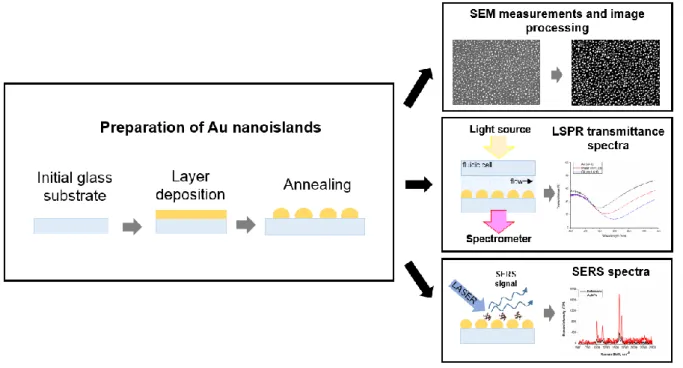
For nanoparticle fabrication previously cleaned glass slides were coated with gold thin films in various thicknesses (6, 9, 10 and 12 nm) with a vacuum thermal evaporation system. The thickness of the created layers was measured with an Ambios XP-1 profilometer. The thickness was controlled by the amount of evaporated gold wire. The prepared thin films were thermally annealed for given time periods (15, 30, 60 and 120 minutes) at certain temperatures (400, 450, 500 and 550 0C) in a ceramic oven in Ar:H atmosphere. Figure 1 gives an overview of the whole technological and investigation sequence of our experiments.
The surface of the obtained AuNP samples was investigated in different places with a Scanning Electron Microscopy (SEM) (Hitachi S-4300) with certain magnification. The SEM images were analyzed by National Instruments Vision Assistant software and the average size of the created AuNPs was calculated based on the obtained data. The average interparticle distance was calculated by a Matlab code using the images created by the Vision Assistant. Only average particle distances less than 100 nm were taken into consideration by the custom image processing software, since our previous modeling and simulation on interparticle plasmon coupling showed,
that this phenomenon becomes most significant below this threshold [24]. Optical transmittance of the created AuNPs was measured using a Shimadzu UV-3600 spectrophotometer.
The LSPR measurements were performed with an Ocean Optics Red Tide USB650 fiber optical spectrophotometer and halogen light source between 400 and 800 nm.
Figure 1 Comprehensive illustration of the nanoparticle preparation technology (layer deposition with thermal evaporation and thermal annealing) and the characterization methods (SEM, transmittance-mode spectrophotometry and SERS) used in this study.
SERS measurements were carried out with a Renishaw 1000 micro-Raman spectrometer. The 514 nm line of an Ar ion laser was used for the excitation, and the excitation spot was focused into a spot having a diameter of 1 micron. The spectra were recorded with 10 s integration time. The SERS enhancement was tested using benzophenone-isopropyl alcohol solution, by dripping the same volume onto the substrate so that the same drop covered partially both the nanoparticle coated region and the clean glass substrate. The latter was used for the reference measurements.
3. Results and Discussion
3.1. Investigation of the prepared gold nanoislands
The freshly prepared AuNPs were investigated by SEM and with an optical spectrophotometer. The SEM images were analyzed and the average island size (equivalent circle diameter) and average separation between the particles – as the two most important parameters of the samples – were obtained. Figure 2a, b, c and d show the influence of different parameters of fabrication technology on the size and separation between the nanoparticles, and on their transmittance spectra as well. The following samples are shown on this figure: 1 – initial thickness 9 nm,thermally annealed at 550 0C for 30 minutes, 2 – initial thickness 10 nm, thermally annealed at 550 0C for 30 minutes, 3 – initial thickness 12 nm, thermally annealed at 550 0C for 30 minutes, It was established that by increasing the initial layer thickness, the size and separation between the particles increase, and their plasmon peak shifts toward longer wavelengths.
3.2. LSPR investigation
The plasmonic performance of the prepared samples was measured by optical spectrophotometry, by changing the medium above the nanoparticles between air (n = 1) and water (n = 1.33) respectively. The measured red shift of the absorbance peak divided by the changes in the refractive index is defined as the bulk refractive index sensitivity (S, [nm/RIU]).
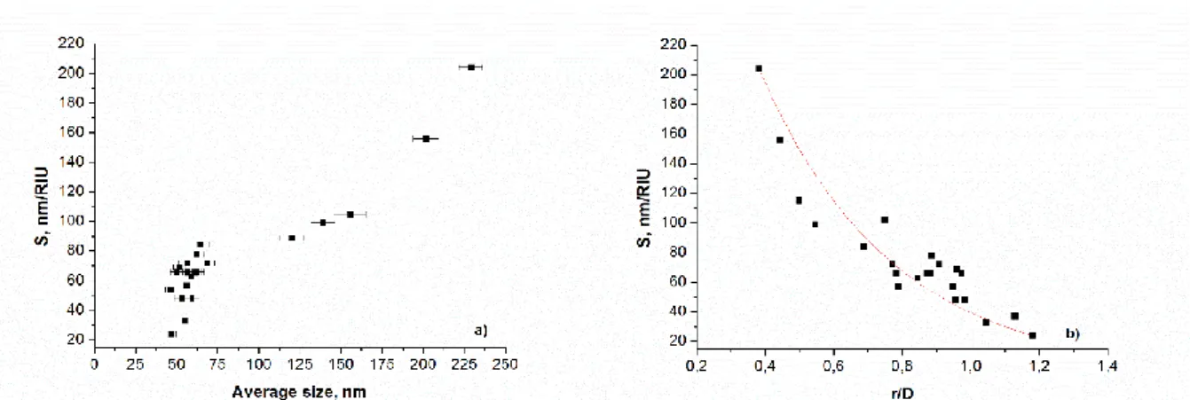
Figure 3a shows typical transmittance spectra illustrating the red shift of the absorbance peak due to the changes in the refractive index of the medium for the AuNPs sample, which SEM images were presented in Figure 2. The main goal of our investigation was to determine the relationship between the average particle size, average interparticle distance and the obtained bulk refractive index sensitivity of the samples. As can be seen in Figure 4a, by increasing the size of the islands the sensitivity also increases. However, the higher particle size shifts the absorbance peak of the spectrum into the red or even near-infrared region (this is especially true for islands with diameter above 150 nm, as can be seen in Figure 4b), which is not desirable for our applications (biosensors). A possible solution would be to keep the particle size at a reasonably large diameter and decrease the average separation between the particles. It is known that decreasing the distance between two nanoparticles leads to a significantly increased near field intensity between the particles due to interparticle plasmon coupling effects [26].
It was also shown previously both experimentally and by modeling, that by tuning these two parameters (particle size and shape) the plasmonic sensitivity of multi-particle systems can be influenced and ideally, optimized [27- 29]. As it can be seen in Figure 4b, the sensitivity depends on the ratio between the particle separation/particle size (marked as r/D) in an exponential way. This exponential dependence can be related to photon tunneling between the coupled nanoparticles and is in good agreement with previous experimental [26, 29] and theoretical reports [24-26] on the subject.
Figure 2. Investigation of the prepared gold nanoislands: a), b), and c) original SEM image of the samples1, 2 and 3, d) The corresponding optical transmittance spectra of the samples.
Based on the results, the main strategies to optimize the plasmonic sensitivity of thermally generated nanoislands could be the following: 1) increase the size of the nanoparticles, keeping in mind also the red shift of the initial absorbance peak, and 2) decrease the interparticle separation between the particles. Based on Figures 3 and 4, an optimal solution can be reached with particle diameters around 150 nm. Here, the initial absorbance peak
of the sensor in the air is still below 600 nm (Figure 3b), with a sensitivity of around 100 nm/RIU and a corresponding r/D of 0.5. Higher sensitivities (and lower r/D ratios) were only reached with larger particles, however, the initial absorbance peak of these particles was above 700 nm in air.
Three main technological parameters that influence the size and distance between the created AuNPs are the initial thickness of the gold layer, annealing temperature and time. Higher initial thickness with the same annealing parameters results in larger nanoparticles and higher sensitivity as it could be seen in Figure 5a. To determine the dependence of the sensitivity on the annealing temperature and time, samples with 9 nm initial layer thickness were annealed at 4 different temperatures for 4 different time periods. Figure 5b shows that higher annealing temperatures and longer annealing times lead to more defined particles (due to Ostwald-ripening) which result in increased gap sizes and thus smaller refractive index sensitivities. So it can be concluded that different time periods should be chosen at different temperatures in order to gain higher sensitivity: at a lower temperature - longer annealing times, at higher temperature shorter annealing times.
Figure 3. a) LSPR transmittance shift of the AuNP sample measured in air (n=1) and water (n=1.33), respectively, Δλ=28nm, Δλ/Δn=84.08nm/RIU. b) The position of the absorbance peak in function of the average particle size of the created AuNPs.
Figure 4. LSPR transmittance shift dependence on the a) average size of the AuNPs (D) and b) the ratio of average particle distance to average particle size (r/D) of the AuNPs.
Figure 5. LSPR transmittance shift dependence on the a) initial layer thickness of the sample heat treated at 550
0C for different annealing time periods and on the b) annealing temperature for the layer with 9 nm initial layer thickness heat treated at different annealing temperatures for different annealing time periods.
Two important conclusions, which transpire from the results are the following: 1) by increasing the deposited thin film layer thickness and thus the resulting nanoisland size the refractive index sensitivity increases; 2) by increasing the annealing time the sensitivity for a given initial layer thickness decreases due to longer particle separation distances. Considering high plasmonic sensitivity and short initial absorbance peak position as our main requirements, the LSPR sensor performance was obtained by annealing a 9 nm thick gold layer for 15 min at 550 oC.
3.3 SERS measurement
Figure 6 compares the normal Raman and the typical SERS spectrum of the same analyte obtained on the AuNPs sample, which SEM images were presented in Figure 2. The highest observable increase in the intensity due to SERS is around 6x of the normal Raman signal on the figure, however, this comparison with the reference spectrum does not reflect the exact SERS enhancement values. While the enhancement occurs only in a close vicinity of the nanoislands, there is a significant non-SERS contribution from other regions of the sample in the SERS spectrum too, influencing the intensity ratios and their comparison. Therefore, the analysis was focused on the relative SERS enhancement factors of the different samples.
Figure 6. Comparison of the 514 nm excited SERS and normal Raman spectra of the test analyte (benzophenone- isopropyl alcohol) in the air.
The main goal of our investigation was to determine the relationship between the average particle size, average particle distance and the obtained SERS efficiency of the samples. It was also shown previously by modeling, that tuning these two parameters (particle size and shape) the Raman intensity can be influenced and ideally, optimized [30,31]. Figure 7 shows the dependence of the relative SERS enhancement factor on the two substrate parameters.
As it can be seen in Figure 7a, with increasing nanoparticle size the Raman enhancement increases, too. However, for particle size above 150 nm, no remarkable SERS enhancement was observed, which is due to the plasmon resonance maximum frequency of these samples, being well above 700 nm. In addition, Figure 7b indicates that the Raman enhancement depends on the ratio of particle separation/particle size (marked as r/D) as well, and the lower the average interparticle distance, the higher the SERS efficiency.
Figure 7. Dependence of the relative SERS enhancement, determined for the 1605 cm-1 peak on the a) average size of the AuNPs (D) and on the b) average particle distance to average particle size ratio (r/D) of the AuNPs.
The above observations can be related to plasmonic properties of the AuNP samples. As it was seen in Fig. 3b, the plasmon resonance wavelength increases with particle size, but for nanoparticle sizes, up to 150 nm, it remains between 500-580 nm. In our measurements, the Raman scattering was excited with 514 nm and the absolute wavelength of the Raman peak used for the SERS enhancement factor determination (at 1605 cm-1) is 560 nm.
Both values are in the range of the absorption maxima of AuNPs and, depending on their relationship, plasmonic enhancement of the excitation or scattered light, or both can occur. The role of interparticle distance can be related to the significantly increased near field intensity between close plasmonic particles due to interparticle plasmon coupling effects [26]. On the other hand, in addition to plasmonic properties, larger and more densely packed nanoparticles have higher specific surface coverage and so higher number of hotspots involved in the SERS enhancement.
Figure 8. Dependence of SERS enhancement ratio of the 1605 and 1664 cm-1 peaks (I1605/I1664) on the wavelength of absorbance peak maximum for the different AuNPs substrates.
Obviously, the obtained SERS enhancement on a particular substrate strongly depends on the relation of the excitation laser, Raman peak, and plasmon resonance wavelengths. While one would expect the maximum SERS
enhancement for zero wavelength difference, with the excitation source, the highest experimental enhancement ratios were obtained when the plasmon resonance was red shifted compared to the excitation wavelength [32]. The reason for this is that in the latter case both the excitation and the Raman scattering could be enhanced by the localized surface plasmons. When measuring Raman spectrum over a broad wavelength range, the width of the plasmon resonance peak becomes an important factor, too, since it will determine the enhancement level of the Raman peaks at different wavenumbers. In order to study these effects, the SERS enhancement factors were determined for two different wavenumbers, at 1605 and 1664 cm-1, corresponding to 560 and 562 nanometers.
Figure 8 shows the dependence of the SERS enhancement ratios of the two peaks on the wavelength of the plasmon resonance peak maximum. It can be seen that with increasing absorption maximum position the relative intensity of the two peaks, located only 2 nm from each other, slowly increases. Up to peak positions of 560 nm, this is obvious, since in this case, the 1605 cm-1 peak is closer to the maximum of plasmon resonance than the 1664 cm-
1 one, and so it should have better enhancement. However, the tendency continues even above 560 nm. According to Fig. 3a the absorbance peak of these substrates is relatively broad, a particular sample with plasmon resonance maximum around 550 nm still can enhance the field of the excitation laser at 514 nm to some extent, and this contribution can affect the relative enhancement ratios.
The analysis of the SERS enhancement of AuNP samples of different morphology shows that both nanoisland size and interparticle distance affect the efficiency of the substrates. Larger and more densely packed gold nanoparticles will result in better SERS performance, which is in good correlation with the findings of the LSPR measurements. It was found also, that in addition to the excitation wavelength, the Raman wavenumber region to be detected should also be taken into account when fabricating and selecting the AuNP substrate for SERS. On the other hand, finding more appropriate excitation energy for a particular AuNP substrate, based on its plasmonic properties, is another option that can be considered for efficient SERS measurements.
By comparing the results obtained by LSPR and SERS tests we can say that effectivity of the two methods in function of the particle parameters are strongly connected. Larger particle sizes also lead to higher LSPR sensitivity and SERS enhancement, while decreasing the gap between the particles are likewise beneficial for both methods.
AuNP substrates showing good performance in both LSPR spectroscopy and SERS could serve a good basis for the fabrication of combined LSPR-SERS sensor devices.
Conclusions
The performance of thermally generated pure gold nanoparticles for LSPR and SERS sensing applications was investigated. The generated nanoisland arrangements were studied with SEM, the parameters of AuNPs were calculated and were compared to their sensing properties. We found that higher deposited layer thicknesses and shorter annealing times lead to higher LSPR bulk refractive index sensitivities which are strongly connected to the increased island sizes and smaller gap distances. SERS measurements performed on the AuNPs gave similar results. Based on the findings, the main strategies of the optimization of the plasmonic sensitivity and surface enhancement of thermally generated gold nanoparticles can be the following: 1) increase the size of the nanoparticles with thicker initial layers (with respect to the significant red shift of the absorbance peak above 150 nm diameter, which should be considered for plasmonic applications), and 2) decrease the interparticle separation between the particles with shorter annealing times.
Acknowledgements
This work was supported by the TÁMOP 4.2.4.A/2-11-1-2012-0001 (Nemzeti Kiválóság Program) and the TÁMOP 4.2.2.A-11/1/KONV- 2012-0036 Project, which is co-financed by the European Union and European Social Fund. The authors acknowledge the financial support by the grant GINOP- 2.3.2-15-2016-00041.
Attila Bonyár and Miklós Veres are grateful for the support of the János Bolyai Research Scholarship of the Hungarian Academy of Sciences. Istvan Csarnovics is grateful for the support through the New National Excellence Program of the Ministry of Human Capacities.
References
1. S. A. Maier, Plasmonics: Fundamentals and Applications, Springer, 2007.
2. S. Zeng, X. Yu, W.-Ch. Law, Y. Zhang, R. Hu, X.-Q. Dinh, H.-P. Ho, K.-T. Yong, Size dependence of Au NP-enhanced surface plasmon resonance based on differential phase measurement, Sensors and Actuators B: Chemical, 176 (2013) 1128.
3. E. Ozbay, Plasmonics: Merging Photonics and Electronics at Nanoscale Dimensions, Science 311 (2006) 189–193.
4. Q. Quayang, S. Zeng, L. Jiang, L. Hong, G. Xu, X.-Q, Dinh, J. Qian, S. He, J. Qu, P. Coquet, K.-T. Yong, Sensitivity enhancement of transition metal dichalcogenides/silicon nanostructure-based sruface plasmon resonance biosensor, Sci. Rep. 6 (2016) 28190.
5. M. Pulu, C. Bala, SPR and SPR imaging: recent trends in developing nanodevices for detection and real- time monitoring of biomolecular events, Sensors, 16 (2016) 870.
6. A. Bonyár, H. Sántha, B. Ring, G. Harsányi, A custom-developed SPRi instrument for biosensor research, Springer Verlag (2012) 1050-1053.
7. Ch. L. Wong, M. Olivo, Surface plasmon resonance imaging sensors: A review, Plasmonics, 9 (2014) 809-824.
8. G. X. Du, T. Mori, M. Suzuki, S. Saito, H. Fukuda, M. Takashi, Evidence of localised surface plasmon enhaned magneto-optical effect in nanodisk array, Appl. Phys. Lett. 96 (2010) 081915.
9. J. Zhao, X. Zhang, CR. Yonzon, AJ. Haes, RP. Van Duyne, Localised surface plasmon resonance biosensors, Nanomedicine, 2 (2006) 219-228.
10. Y. Gao, Q. Gan, F. Bartoli, Breakthroghs in photonics 2013: research highlights on biosensors based on plasmonic nanostructures, IEEE Photonics Journal, 6 (2014) 1-5.
11. S. Link, M. A. El-Sayed, Shape and sized dependence of radiative, non-radiative and photothermal properties of gold nanocrystals, Int. Reviews in Physical Chemistry, 19 (2000) 409-453.
12. Celso de Mello Donegá, Nanoparticles, Springer, 2014.
13. A. Bonyár, T. Lednicky, J. Hubálek, LSPR nanosensors with highly ordered gold nanoparticles fabricated on nanodimpled aluminium templates, 30th Eurosensors Conference, EUROSENSORS 2016, Procedia Engineering, 168 (2016) 1160-1163.
14. G. A. Lopez, M.-C. Estevez, M. Soler, L.M. Lechuga, Recent advances in nanoplasmonic biosensors:
applications and lab-on-chip integration, Nanophotonics, 6 (2017) 123-136.
15. K. A. Willets, R. P. Van Duyne (2007): Localized surface plasmon resonance spectroscopy and sensing, Annual Review of Physical Chemistry, Annual Reviews, 267-297.
16. A. Dimitrev, Nanoplasmonic Sensors, Springer, 2012.
17. A.V. Kabashin, P. Evans, S. Pastkovsky, W. Hendren, G.A. Wurtz, R. Atkinson, R. Pollard, V.A.
Podolskiy, A.V. Zayats, Plasmonic nanorod metamaterials for biosensing, Nature materials, 8 (2009) 867-871.
18. A. Serrano, O. Rodríguez de la Fuente, M. A. García, Extended and localized surface plasmons in annealed Au films on glass substrates. Journal of Applied Physics 108 (2009) 074303.
19. K. Kneipp, H. Kneipp, I. Itzkan, R. R. Dasari, M. S. Feld, Surface-enhanced Raman scattering and biophysics, J. Phys. : Condens. Matter, 14 (2002) 597-624.
20. D.A. Stuart, A.J. Haes, C.R. Yonzon, E.M. Hicks, R.P. Van Duyne, Biological applications of localised surface plasmonic phenomenae, IEE Proc Nanobiotechnol. 152 (2005) 13-32.
21. B. Sharma, R.R. Frontiera, A.-I. Henry, E. Ringe, R.P. Van Duyne, SERS: Materials, applications, and the future, Materials Today, 15 (2012) 16-25.
22. K. Kneipp, M. Moskovitz, H. Kneipp, Surface-enhanced Raman scattering, Springer, 2006.
23. Y. Ozaki, K. Kneipp, R. Aroca, Frontiers of surface-enhanced Raman scattering: single nanoparticles and single cells, Willey, 2014.
24. A. Bonyár, Simulation of the refractive index sensitivity of coupled plasmonic nanostructures, 30th Eurosensors Conference, EUROSENSORS 2016, Procedia Engineering, 168 (2016)
25. A. Bonyár, G. Szántó, I. Csarnovics, Coupled surface plasmon on gold nanocubes - an investigation by simulation, Design and Technology in Electronic Packaging (SIITME), 2016 IEEE 22nd International Symposium for (2016) 139-141.
26. K.-H. Su, Q.-H. Wei, and X. Zhang, Interparticle Coupling Effects on Plasmon Resonances of Nanogold Particles. Nano Letters 3 (2003) 1087-1090.e 4
27. Yan (2011), Bo Yan, Svetlana V. Boriskina, and Björn M. Reinhard, Design and Implementation of Noble Metal Nanoparticle Cluster Arrays for Plasmon Enhanced Biosensing, J Phys Chem C Nanomater Interfaces. 115 (2011) 24437–24453.
28. E. Martinsson, B. Sepulveda, P. Chen, A. Elfwing, B. Liedberg, D. Aili, Optimizing the Refractive Index Sensitivity of Plasmonically Coupled Gold Nanoparticles, Plasmonics 9 (2014) 773–780
29. M. Kang, S.-G. Park, K.-H. Jeong, Repeated Solid-state Dewetting of Thin Gold Films for Nanogap-rich Plasmonic Nanoislands, Scientific Reports 5 (2015) 14790.
30. L. Gunnarsson, E. J. Bjerneld, H. Xu, S. Petronis, B. Kasemo, and M. Käll, Interparticle coupling effects in nanofabricated substrates for surface-enhanced Raman scattering, Applied Physics Letters 78 (2001) 35-42.
31. N. D. Israelsen, C. Hanson, E. Vargis, Nanoparticle properties and synthesis effects on surface- enhanced Raman scattering enhancement factor: an introduction, The Scientifit World Journal, 2015 (2015) 124582-124894.
32. A.D. McFarland, M.A. Young, J.A. Dieringer, R.P. Van Duyne, Wavelength-scanned surface- enhanced Raman excitation spectroscopy, J. Phys. Chem. B 109 (2005) 11279.